US20030193512A1 - Image processing device for layered graphics - Google Patents
Image processing device for layered graphics Download PDFInfo
- Publication number
- US20030193512A1 US20030193512A1 US10/392,180 US39218003A US2003193512A1 US 20030193512 A1 US20030193512 A1 US 20030193512A1 US 39218003 A US39218003 A US 39218003A US 2003193512 A1 US2003193512 A1 US 2003193512A1
- Authority
- US
- United States
- Prior art keywords
- image
- source
- combiner
- order
- memory
- Prior art date
- Legal status (The legal status is an assumption and is not a legal conclusion. Google has not performed a legal analysis and makes no representation as to the accuracy of the status listed.)
- Granted
Links
Images


Classifications
-
- G—PHYSICS
- G09—EDUCATION; CRYPTOGRAPHY; DISPLAY; ADVERTISING; SEALS
- G09G—ARRANGEMENTS OR CIRCUITS FOR CONTROL OF INDICATING DEVICES USING STATIC MEANS TO PRESENT VARIABLE INFORMATION
- G09G5/00—Control arrangements or circuits for visual indicators common to cathode-ray tube indicators and other visual indicators
- G09G5/36—Control arrangements or circuits for visual indicators common to cathode-ray tube indicators and other visual indicators characterised by the display of a graphic pattern, e.g. using an all-points-addressable [APA] memory
- G09G5/39—Control of the bit-mapped memory
- G09G5/395—Arrangements specially adapted for transferring the contents of the bit-mapped memory to the screen
- G09G5/397—Arrangements specially adapted for transferring the contents of two or more bit-mapped memories to the screen simultaneously, e.g. for mixing or overlay
-
- G—PHYSICS
- G09—EDUCATION; CRYPTOGRAPHY; DISPLAY; ADVERTISING; SEALS
- G09G—ARRANGEMENTS OR CIRCUITS FOR CONTROL OF INDICATING DEVICES USING STATIC MEANS TO PRESENT VARIABLE INFORMATION
- G09G2340/00—Aspects of display data processing
- G09G2340/10—Mixing of images, i.e. displayed pixel being the result of an operation, e.g. adding, on the corresponding input pixels
Definitions
- the present invention relates to an image processing device for layered graphics and a semiconductor chip implementing that device. More particularly, the present invention relates to an image processing device, as well as to a semiconductor integrated circuit chip, which reads out a plurality of source images from a graphics memory and combines them in a predetermined order to form a single picture.
- Graphics functions employed in some electronic devices take advantages of a multiple-layer structure of graphics data, where a picture is represented as a set of overlaid images that are each rendered on separate virtual drawing sheets, or layers.
- a picture is represented as a set of overlaid images that are each rendered on separate virtual drawing sheets, or layers.
- the layered graphics one can modify a particular graphical element in a picture by replacing the corresponding layer with another one.
- a new element can be added to an existing picture by inserting a new layer.
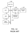
- FIG. 12 shows a typical configuration of electronic equipment having conventional graphics display functions.
- the illustrated equipment is composed of the following elements: a host central processing unit (host CPU) 100 , a read only memory (ROM) 101 , a random access memory (RAM) 102 , input devices 103 , a graphics chip 104 , a graphics memory 105 , a host CPU bus 106 , and a monitor unit 107 .
- the host CPU 100 performs various operations according to the programs stored in the ROM 101 or RAM 102 , besides controlling other part of the equipment.
- the ROM 101 stores basic programs and data that the host CPU 100 executes and manipulates.
- the RAM 102 serves as temporary storage for application programs and scratchpad data that the host CPU 100 executes and manipulates at runtime.
- the input devices 103 include a pointing device that generates signals representing user operations.
- the graphics chip 104 produces each layer image according to drawing commands issued by the host CPU 100 , and combines those images into a single picture for display on the monitor unit 107 .
- the graphics memory 105 stores those images and feeds them back to graphics chip 104 when so requested.
- the host CPU bus 106 interconnects the host CPU 100 , ROM 101 , RAM 102 , input devices 103 , and graphics chip 104 , allowing them to exchange information with each other.
- the monitor unit 107 is a display device such as a liquid crystal display (LCD) to show text and graphic images according to video signals supplied from the graphics chip 104 .
- LCD liquid crystal display
- FIG. 13 gives details of the graphics chip 104 used in the electronic equipment of FIG. 12.
- the graphics chip 104 contains the following functional blocks: a video timing generator 10 , memory read units 11 a to 11 d , transparent color registers (TCR) 12 a to 12 d , transparent color discriminators (TCD) 13 a to 13 d , coefficient registers 14 a to 14 d , image combiners 15 a to 15 d , a background color register 16 , a host access controller 17 , and a graphics memory interface 18 .
- TCR transparent color registers
- TCD transparent color discriminators
- the video timing generator 10 produces a vertical synchronization signal, horizontal synchronization signal, and other necessary signals.
- the host CPU 100 specifies the pulse width and cycle period of those synchronization signals by sending parameters over the host CPU bus 106 .
- Four memory read units 11 a to 11 d read out image data of each layer from the graphics memory 105 in burst transfer mode via the graphics memory interface 18 . They also serve as buffer storage in delivering image data to its destination, outputting the contents at a signal rate that is suitable for the display device used.
- the transparent color registers 12 a to 12 d define which color code in a picture will be interpreted as a “transparent color.”
- the host CPU 100 sets these registers via the host CPU bus 106 .
- the transparent color discriminators 13 a to 13 d compare each pixel of incoming image data with the color code stored in the corresponding transparent color register. If a match is found, that pixel should be regarded as transparent.
- the image combiners 15 a to 15 d are informed of this transparency test result in an extended bit of image data.
- the coefficient registers 14 a to 14 d have a width of, for example, eight bits to hold “blending coefficients” given by the host CPU 100 via the host CPU bus 106 . Those blending coefficients, along with the transparency test results, are supplied to the image combiners 15 a to 15 d in other extended bits of image data.
- Each image combiner 15 a to 15 d combines a source image supplied from its corresponding memory read unit 11 a to 11 d with a lower-layer combined image produced by the preceding image combiner. They have two operation modes: “transparent color mode” and “blend mode.” In transparent color mode, the image combiners 15 a to 15 d select either a given source image sent from their corresponding memory read units 11 a to 11 d or the combined image of lower layers, depending on the transparency test result about each pixel of the source image. Accordingly, when a layer image has a transparent region, the image combiners 15 a to 15 d pass lower-layer pixels to the next layer, allowing lower layers to be seen through upper layers of the picture. In blend mode, on the other hand, two images are added with certain weighting factors that are defined as the blending coefficients mentioned above.
- the background color register 16 stores a color code that represents the color of a background plane.
- the host access controller 17 aids the host CPU 100 to make access to the graphics memory 105 . Through this host access controller 17 , the host CPU 100 supplies rendered image data for display.
- the graphics memory interface 18 is responsible for arbitration of access requests to the graphics memory 105 , which are issued from the memory read units 11 a to 11 d and host access controller 17 . It controls actual memory read/write cycles, accepting one request at a time.
- the conventional graphics chip 104 operates as follows. Suppose here that a set of layered images are stored in areas A to D of the graphics memory 105 to produce a combined picture in transparent color mode. Transparent areas of each layer image are encoded with a special color code, while other opaque areas have ordinary color code values in their pixels.
- the fourth memory read unit 11 d for the bottom-most layer is set up with the start address of area D in the graphics memory 105 .
- the fourth memory read unit lid reads out a predetermined amount of image data from area D, stores the data in its internal buffer (e.g., FIFO buffer), and outputs it to the corresponding image combiner 15 d as requested.
- This data is also supplied to the transparent color discriminator 13 d , which compares each incoming pixel with the code stored in the transparent color register 12 d . If they match each other, the transparent color discriminator 13 d records it in an extension bit of that pixel.
- the fourth image combiner 15 d combines the output of the background color register 16 with the image data supplied from the fourth memory read unit 11 d . More specifically, the fourth image combiner 15 d selects the background color code for picture areas that the transparent color discriminator 13 d has determined to be transparent, while it selects the output of the fourth memory read unit 11 d for the remaining areas. In this way, the graphics chip 104 combines the given area-D image with a background plane in transparent color mode.
- the next memory read unit 11 c set up with the start address of area C, reads out a predetermined amount of image data from the area C when its access request is granted by the graphics memory interface 18 .
- the third memory read unit 11 c stores the data in its integral buffer for use in the corresponding image combiner 15 c .
- the transparent color discriminator 13 c compares each pixel supplied from the memory read unit 11 c with a code stored in the transparent color register 12 c . If they match each other, the transparent color discriminator 13 c records it in an extended bit of that pixel.
- the third image combiner 15 c chooses the output of the preceding image combiner 15 d for image segments that the transparent color discriminator 13 c has found it transparent, while selecting the output of the third memory read unit 11 c for the remaining segments.
- the two image combiners 15 d and 15 c have thus combined the area-D and area-C images in transparent color mode, and just in the same way, the next two image combiners 15 b and 15 a overlay area-B and area-A images on the outcome of the third image combiner 15 c.
- the architecture described above is unable to exchange one layer with another with a simple command, since it requires a memory-to-memory transfer of image data or reconfiguration of address parameters in the memory read units 11 a to 11 d . That is, the conventional layered graphics device architecture lacks flexibility in reordering the layers in a picture.
- an image processing device which produces a picture by combining layered images stored in a memory.
- This device comprises the following elements: a reading circuit which reads out a plurality of source images from the memory; a combiner which combines the source images provided by the read circuit in a specific order; and a combination order controller, disposed between the reading circuit and combiner circuit, which determines in what order the source images are combined by the combiner circuit.
- FIG. 1 is a conceptual view of the present invention
- FIG. 2 is a block diagram showing an embodiment of the present invention
- FIG. 3 shows the details of a graphics chip used in the equipment of FIG. 2;
- FIG. 4 shows the details of memory read units used in the graphic chip of FIG. 3;
- FIG. 5 shows the details of image combiners used in the graphic chip FIG. 3;
- FIGS. 6 (A) and 6 (B) show an example of image data stored in memory areas D and C, respectively;
- FIGS. 7 (A) and 7 (B) show an example of image data stored in memory areas B and A, respectively;
- FIG. 8 represents the format of a selection control word stored in selection registers shown in FIG. 3;
- FIG. 9 shows what is associated with each field value in the selection control word of FIG. 8;
- FIG. 10(A) represents a picture produced by combining a background image with the area-D image of FIG. 6(A);
- FIG. 10(B) represents a picture produced by combining the area-C image of FIG. 6(B) with the picture of FIG. 10(A);
- FIG. 11(A) represents a picture produced by combining the area-B image of FIG. 7(A) with the picture of FIG. 10(B);
- FIG. 11(B) represents a picture produced by combining the area-A image of FIG. 7(B) with the picture of FIG. 11(A);
- FIG. 12 shows a typical configuration of electronic equipment having conventional graphics display functions
- FIG. 13 gives details of a conventional graphics chip used in the equipment shown in FIG. 12.
- FIG. 1 is a conceptual view of the present invention.
- the proposed image processing device comprises a memory 1 , a reading circuit 2 , a combination order controller 3 , and a combiner circuit 4 .
- the memory 1 has a plurality of predetermined storage areas each containing one layer of image data.
- the reading circuit 2 reads them out of the memory 1 as source images for a final picture.
- the combiner circuit 4 contains a plurality of image combiners cascaded one after another to combine the plurality of source images provided from the reading circuit 2 in a predetermined order.
- the combination order controller 3 disposed between the reading circuit and combiner circuit, determines which source image to supply to each image combiner, thereby controlling the order of layers to be combined by the combiner circuit 4 .
- the above system operates as follows.
- a plurality of source images are kept in the memory 1 , each corresponding to a particular layer of a picture.
- This layer assignment has to be flexible.
- the reading circuit 2 reads out a predetermined amount of image data D, C, B, and A in that order and supplies it to the combination order controller 3 .
- the combination order controller 3 determines to which image combiner each source image should go, according to a given control word.
- This control word is stored in, for example, a register that can be set by an external entity. In the present case, this control word register specifies that the images D, C, B, and A be combined in that order.
- the combiner circuit 4 has an array of four image combiners, which are referred to herein as the first to fourth image combiners, the first being placed at the top-most layer.
- the combination order controller 3 directs the image D to the fourth image combiner, C to the third image combiner, B to the second image combiner, and A to the first image combiner.
- a background image is also supplied to the fourth image combiner as an underlying plane below the bottom layer image.
- the fourth image combiner combines the background image and the bottom-most layer image D and supplies the resulting combined image to the third image combiner.
- the third image combiner combines the next layer image C with the fourth combiner's output and supplies the resulting image to the second image combiner.
- the second image combiner combines the next layer image B with the third combiner's output and supplies the resulting image to the first image combiner.
- the first image combiner combines the top layer image A with the second combiner's output, thus obtaining a completely combined picture as its final output.
- the order of image combination has to be changed, it can be done by simply writing a new value to the control word register in the combination order controller 3 .
- the combination order controller 3 begins directing the four source images to their new destinations, thereby changing the order of layers.
- a new image order (C, D, A, B) is now specified, instead of the initial one (D, C, B, A), in the control word register.
- the combination order controller 3 directs the image C to the fourth image combiner, D to the third image combiner, A to the second image combiner, and B to the first image combiner.
- the fourth image combiner combines the background image with the bottom-most layer image C and supplies the combined image to the third image combiner.
- the third image combiner combines the next-to-bottom layer image D with the fourth combiner's output, and the second image combiner combines the next layer image A with the third combiner's output.
- the first image combiner combines the top-most layer image B with the second combiner's output, thus obtaining a new picture composed of four source images stacking in the order of C, D, A, and then B.
- the present invention employs a combination order controller 3 to rearrange the order of source images provided by the reading circuit 2 , before supplying them to the combiner circuit 4 .
- This feature of the present invention makes it easy to change the combination order.
- FIG. 2 shows a typical configuration of electronic equipment using a graphics chip according to the present invention.
- the proposed equipment is composed of the following blocks: a host central processing unit (host CPU) 100 , a read only memory (ROM) 101 , a random access memory (RAM) 102 , input devices 103 , a graphics chip 104 , a graphics memory 105 , a host CPU bus 106 , and a monitor unit 107 .
- the proposed equipment is similar to the conventional equipment explained earlier in FIG. 12, except that it employs an improved graphics chip 200 , instead of a conventional one 104 .
- the host CPU 100 performs various operations according to programs stored in the ROM 101 or RAM 102 , besides controlling other part of the equipment.
- the ROM 101 stores basic programs and data that the host CPU 100 executes and manipulates.
- the RAM 102 serves as temporary storage for application programs and scratchpad data that the host CPU 100 executes and manipulates at runtime.
- the input devices 103 include a pointing device that generates data signals representing user operations.
- the graphics chip 200 produces a graphic image of each layer according to drawing commands sent from the host CPU 100 , and combines those layer images into a single picture for display on the monitor unit 107 . When the host CPU 100 requests a change in the order of images, the graphics chip 200 reconfigures itself to produce a picture according to the new order specified.
- the graphics memory 105 stores multiple source images that graphics chip 200 has rendered, being ready for feeding them back to graphics chip 200 when so requested.
- the host CPU bus 106 interconnects all the above functional blocks, allowing them to exchange data, directly with each other or with the intervention of the host CPU 100 .
- the monitor unit 107 is, for example, a liquid crystal display (LCD) to show text and graphic images according to the video signals supplied from the graphics chip 200 .
- FIG. 3 gives details of the graphics chip 200 used in the equipment of FIG. 2.
- the graphics chip 200 has the following functional blocks: a video timing generator 10 , memory read units 11 a to 11 d , transparent color registers (TCR) 12 a to 12 d , transparent color discriminators (TCD) 13 a to 13 d , coefficient registers 14 a to 14 d , image combiners 15 a to 15 d , a background color register 16 , a host access controller 17 , a graphics memory interface 18 , layer selectors 30 a to 30 d , and selection registers 31 a to 31 d .
- This circuit has some elements and wiring for them that are absent in the conventional chip discussed in FIG. 13. They are: layer selectors 30 a to 30 d and selection registers 31 a to 31 d.
- the above-listed blocks are designed to function as follows.
- the video timing generator 10 produces a vertical synchronization (VSYNC) signal, horizontal synchronization (HSYNC) signal, and other necessary signals for display control, where the host CPU 100 specifies the pulse width and cycle period of each signal by sending parameters over the host CPU bus 106 .
- VSYNC vertical synchronization
- HSELNC horizontal synchronization
- the memory read units 11 a to 11 d read out a source image of each layer from the graphics memory 105 in burst transfer mode via the graphics memory interface 18 . They also serve as buffer storage for outputting the image data at a data rate that is suitable for the display device used. The structure of those memory read units 11 a to 11 d will be discussed in greater detail later.
- the transparent color registers 12 a to 12 d define which color code in a picture shall be treated as a “transparent color.”
- the host CPU 100 sets those registers via the host CPU bus 106 .
- the transparent color discriminators 13 a to 13 d compare every pixel of an incoming image with the color code stored in the corresponding transparent color register. If a match is found, that pixel should be treated as a transparent pixel. This transparency test result is supplied to the image combiners 15 a to 15 d in an extended bit attached to each image data word.
- the coefficient registers 14 a to 14 d have a width of, for example, eight bits to hold blending coefficients given by the host CPU 100 via the host CPU bus 106 . Those blending coefficients are sent, along with the transparency test results, to the image combiners 15 a to 15 d in another set of extended bits of image data.
- the four image combiners 15 a to 15 d are cascaded, one on top of another, to combine source image data read by their corresponding memory read units 11 a to 11 d with lower layer images. They have two distinct operation modes: transparent color mode and blend mode. In transparent color mode, the image combiners 15 a to 15 d select either a given source image sent from their corresponding memory read units 11 a to 11 d or the combined image of lower layers, depending on the transparency test result about each pixel of the given source image. Accordingly, when a source image has a transparent region, the image combiners 15 a to 15 d pass lower-layer pixels to the next layer, allowing lower layers to be seen through upper layers of the picture.
- transparent color mode the image combiners 15 a to 15 d select either a given source image sent from their corresponding memory read units 11 a to 11 d or the combined image of lower layers, depending on the transparency test result about each pixel of the given source image. Accordingly, when a source image has a transparent region, the image combiners 15
- blend mode on the other hand, two given source images are added together with certain weighting factors defined as the blending coefficients mentioned above. More specifically, they are blended into one picture according to the following formula:
- Output Image (Source Image) ⁇ R+(Lower-Layer Image) ⁇ ( 1 ⁇ R )
- R represents a blending coefficient.
- R 0.25
- the present source image and lower-layer image are mixed at a ratio of 1:3 as follows.
- the background color register 16 stores a fixed color code that is provided to the bottom-layer image combiner as a background plane lying under the bottom layer image.
- the host access controller 17 aids the host CPU 100 to make access to the graphics memory 105 when rendering source images for display.
- the graphics memory interface 18 is responsible for the arbitration between concurrent access requests to the graphics memory 105 from the memory read units 11 a to 11 d , as well as from the host access controller 17 . It controls actual memory read/write cycles, accepting one request at a time.
- the layer selectors 30 a to 30 d choose one of the outputs of the memory read units 11 a to 11 d according to the information stored in their associated selection registers 31 a to 31 d , thus providing each corresponding image combiner 15 a to 15 d with a selected source image.
- the selection registers 31 a to 31 d set by the host CPU 100 , specify which source image to supply to each layer selector 30 a to 30 d.
- FIG. 4 gives details of the memory read units 11 a to 11 d .
- the memory read units 11 a to 11 d each have the following elements: a start address register 300 , a stride register 301 , an adder 302 , a selector 303 , a raster address register 304 , a pixel address counter 305 , a controller 306 , and a first-in first-out (FIFO) buffer 307 .
- the start address register 300 holds the start address of an image storage area.
- the stride register 301 contain a constant value that is used as an increment when the circuit calculates a new raster address.
- the host CPU 100 sets those two registers through the host CPU bus 106 .
- the adder 302 calculates the sum of the values stored in the stride register 301 and raster address register 304 and supplies the result to the selector 303 .
- the selector 303 chooses the former when the circuit attempts access to the top address of the assigned memory area, while otherwise selecting the latter. The output of this selector 303 is directed to the raster address register 304 .
- the raster address register 304 holds the start address of each scan line, or raster, of an image, which is loaded with the value of the start address register in synchronization with the VSYNC signal and incremented by the value of the stride register 301 each time an HSYNC pulse comes.
- the pixel address counter 305 generates pixel address for scanning every pixel in an image along each raster. It is loaded with a raster start address from the raster address register 304 in synchronization with the HSYNC signal, and afterward, incremented by one as the scanning proceeds. The output of this pixel address counter 305 is used to read the graphics memory 105 .
- the controller 306 sends an access request signal to the graphics memory interface 18 , according to the state of VSYNC and HSYNC signals and FIFO buffer 307 . In response to the request, the graphics memory interface 18 returns an access acknowledge signal back to the controller 306 .
- the controller 306 also produces signals to control the selector 303 , raster address register 304 , and pixel address counter 305 .
- the FIFO buffer 307 stores a plurality of memory data words in the order that they are read out of the graphics memory 105 and outputs them in the same order.
- the graphics memory 105 outputs data in high-speed burst transfer mode. Because of the intermittent nature of those bursts, the circuit has to employ some buffer storage for rectify the flow of data, not to disrupt the image displayed on the screen.
- the FIFO buffer 307 as temporary storage, smoothes out bursty data flow from the graphics memory 105 , thus supplying data in phase with the video timings.
- FIG. 5 gives details of the image combiners 15 a to 15 d shown in FIG. 3.
- the image combiners 15 a to 15 d each comprise: a complement operator 400 , multipliers 401 and 402 , and an adder 403 , and selectors 404 and 405 .
- the complement operator 400 extracts a blending coefficient from an extended part of image data and calculates the complement of that coefficient value. This complement operation yields the term (1 ⁇ R) for a given coefficient value of R.
- the first multiplier 401 multiplies lower-layer image data (i.e., output of the immediately preceding image combiner) by the complement of the given blending coefficient.
- the second multiplier 402 multiples source image data supplied from the memory read units 11 a to 11 d by the blending coefficient R. Now that the two multipliers have weighted the source image and lower-layer image by the blending coefficient and its complement, respectively, then the adder 403 sums up the two multiplier outputs. In this way, an image blending process is accomplished by the complement operator 400 , multipliers 401 and 402 , and adder 403 .
- the first selector 404 selects lower-layer image data if the present source image is transparent, and if not, it lets the present source image through.
- the first selector 404 makes this selection on an individual pixel basis, consulting the transparency test result found in an extended part of image data.
- the second selector 405 chooses the output of the first selector 404 when the operation mode selection signal from the host CPU 100 indicates transparent color mode. In blend mode, it selects the output of the adder 403 . The image selected as such is then supplied to the next-layer image combiner.
- FIG. 6(A) in area D
- FIG. 6(B) in area C
- FIG. 7(A) in area B
- still another image of FIG. 7(B) in area A the host CPU 100 supplies the image combiners 15 a to 15 d with a signal indicating transparent color mode, making the second selector 405 choose the output of the first selector 404 .
- the host CPU 100 then sets up the selection registers 31 a to 31 d with a selection control word shown in FIG. 8, for example.
- This selection control word is an eight-bit word consisting of four fields, each containing a two-bit code that specifies which source image to supply to the image combiners 15 a to 15 d . More specifically, bit#0 and bit#1 define which image the first image combiner 15 a should process. Likewise, bit#2 and bit#3 are assigned to the second image combiner 15 b , bit#4 and bit#5 to the third image combiner 15 c , and bit#6 and bit#7 to the fourth image combiner 15 d , to determine their source selection.
- FIG. 9 shows the definition of two-bit source selection codes.
- the code “00,” for instance, specifies that the image combiner of interest will receive image data from the first memory read unit 11 a .
- the code “1” designates the second memory read unit 11 b , “10” the third memory read unit 11 c , and “11” the fourth memory read unit 11 d.
- the host CPU 100 has set a binary value of “00011011” to the selection registers 31 a to 31 d .
- the top-most two bits “00” of this value makes the first image combiner 15 a to receive image data from the first memory read unit 11 a (see FIG. 9).
- the next two bits are “01,” which specifies the second memory read unit 11 b as the data source for the second image combiner 15 b .
- the subsequent code “10” makes the third image combiner 15 c receive data from the third memory read unit 11 c
- the lowest two-bit code “11” makes the fourth image combiner 15 d receive data from the fourth memory read unit 11 d.
- the host CPU 100 then gives a transparent color code to each transparent color register 12 a to 12 d , and a background color code to the background color register 16 . Subsequently the host CPU 100 configures the memory read units 11 a to 11 d in such a way that their internal start address registers 300 will point at the top of each image area A to D. That is, the start address of area A is set to the start address register 300 of the first memory read unit 11 a .
- the start address of area B is set to the start address register 300 of the second memory read unit 11 b .
- the start address of area C is set to the start address register 300 of the third memory read unit 11 c .
- the start address of area D is set to the start address register 300 of the fourth memory read unit 11 d .
- the host CPU 100 also sets the raster length in the stride register 301 of each memory read unit 11 a to 11 d.
- the graphics chip 104 starts to produce a combined picture upon completion of the register initialization described above.
- the fourth memory read unit 11 d reads the area-D image data (FIG. 6(A)) from the graphics memory 105 in burst transfer mode. More specifically, the controller 306 in the fourth memory read unit 11 d directs the selector 303 to choose the start address register 300 when VSYNC becomes active. The raster address register 304 is thus loaded with the start address of area D that appears at the output of the selector 303 .
- the pixel address counter 305 This then allows the pixel address counter 305 to receive the area-D start address from the raster address register 304 when the controller 306 issues an access request signal in an attempt to fetch the first part of a relevant source image from the graphics memory 105 .
- the controller 306 performs a handshake with the graphics memory interface 18 , sending a request and receiving an acknowledgement.
- the pixel address counter 305 increments itself by one, thus updating the address output signal.
- the graphics memory 105 supplies a burst of image data to the FIFO buffer 307 through the graphics memory interface 18 .
- the FIFO buffer 307 distributes data to every layer selector 30 a to 30 d at a predetermined rate, in synchronization with the HSYNC signal. The operation of the layer selectors 30 a to 30 d will be described later.
- the controller 306 directs the selector 303 to choose the adder 302 's output, thus incrementing the raster address register 304 by the raster length set in the stride register 301 .
- the updated raster address register 304 now points at the second raster of the area-D source image.
- the pixel address counter 305 thus receives a new value from the raster address register 304 and starts to generate another series of incremental address signals.
- the fourth memory read unit 11 d (FIG. 4) is loaded with the area-D start address at each VSYNC, and that address is incremented by the raster length at every HSYNC.
- the fourth memory read unit 11 d sets its internal address counter in this way and makes access to the graphics memory while incrementing that counter.
- Image data in the FIFO buffer 307 is supplied to the transparent color discriminator 13 d .
- the transparent color discriminator 13 d tests whether each pixel color in the given image data matches the specified transparent color. This transparency test result is recorded as an extended bit of image data for use in the layer selectors 30 a to 30 d , which is therefore referred to as the “transparency test result bit.”
- the layer selectors 30 a to 30 d decode a relevant part of the selection control word stored in the selection registers 31 a to 31 d , thus choosing either of the four sources (memory read units 11 a to 11 d ) to supply their respective image combiners 15 a to 15 d with a source image.
- the fourth layer selector 30 d is supposed to select the fourth memory read unit 11 d as the image source for the fourth image combiner 15 d , as mentioned earlier. Because the graphics chip 200 is operating now in transparent color mode, only the first selector 404 plays an active role in the fourth image combiner 15 d (as well as in the other combiners 15 a to 15 c ).
- This first selector 404 is controlled by the transparency test result bit in the given image data. If that bit indicates transparency, the first selector 404 chooses lower-layer image data (which is given by the background register in the case of the fourth image combiner 15 d ). Otherwise, it chooses the image data given by the fourth layer selector 30 d . Since the area D currently stores an image shown in FIG. 6(A), the fourth image combiner 15 d replaces every hatched segment (i.e., transparent segment) of the image with the background color set in the background color register 16 .
- FIG. 10(A) shows the resultant image, in which the hatching represents the background color.
- the third memory read unit 11 c reads out image data from area C of the graphics memory 105 , which is shown in FIG. 6(B). consulting its corresponding transparent color register 12 c , the transparent color discriminator 13 c tests whether each pixel color in the given image data matches the transparent color specified therein. This transparency test result is recorded in an extended bit of the image data for use in the layer selectors 30 a to 30 d . Since it is designated as the third layer in the present example, the area-C image data, including its transparency test result bit, is directed to the third image combiner 15 c through the third layer selector 30 c .
- the first selector 404 selects either the lower-layer image data given by the fourth image combiner 15 d or the area-C source image given by the third layer selector 30 c , depending on the state of the transparency test result bit.
- the area-C image of FIG. 6(B) has now been overlaid on the lower-layer image of FIG. 10(A), resulting in a combined image of FIG. 10(B).
- the second image combiner 15 b combines the area-B image (FIG. 7(A)) supplied from the second memory read unit 11 b with the output image (FIG. 10(B)) of the third image combiner 15 c .
- the result is shown in FIG. 11(A).
- the first image combiner 15 a then combines the area-A image (FIG. 7(B)) supplied from the first memory read unit 11 a with the output image (FIG. 11 (A)) of the third image combiner 15 c .
- the above steps finally yield a combined picture shown in FIG. 11(B), in which the four layer images in areas D, C, B, and A are overlaid in that order.
- the host CPU 100 is able to implement it immediately by writing a new value to the selection registers 31 a to 31 d .
- the selection registers 31 a to 31 d are loaded with a selection control word (FIG. 8) of “10011100.”
- This control word makes the fourth layer selector 30 d choose the output of the first memory read unit 11 a , the third layer selector 30 c choose the output of the fourth memory read unit lid, the second layer selector 30 b choose the output of the second memory read unit 11 b , and the first layer selector 30 a choose the output of the third memory read unit 11 c .
- the image combiners 15 d to 15 a thus combine those four images in the order of A, D, B, and C.
- the present embodiment permits the host CPU 100 to change the order of layers only by issuing a simple 8-bit control word to update the selection registers 31 a to 31 d.
- blend mode the host CPU 100 configures the second selector 405 in every image combiner 15 a to 15 d in such a way that it will select the adder 403 's output.
- the host CPU 100 further initializes the coefficient registers 14 a to 14 d with appropriate blending factors.
- the selection registers 31 a to 31 d have to be configured previously with a selection control word “00011011” just as in the case of transparent color mode.
- the fourth memory read unit 11 d fetches an image from area D of the graphics memory 105 .
- the coefficient register 14 d appends the blending coefficient to the image data as its extension bits. Being designated as the fourth layer, the area-D image is directed to the fourth image combiner 15 d through the fourth layer selector 30 d .
- the complement operator 400 in the fourth image combiner 15 d extracts a blending coefficient R from the extension bits of the given image data and supplies its output (1 ⁇ R) to the first multiplier 401 .
- the first multiplier 401 multiplies lower-layer image data (i.e., output of the background color register 16 in this case) by the complement (1 ⁇ R) of the given blending coefficient R.
- the second multiplier 402 on the other hand, multiples the source image data supplied from the fourth memory read unit lid by the blending coefficient R.
- the adder 403 then sums up the two multiplier outputs.
- Output Image (Area-D Image) ⁇ R +(Lower-Layer Image) ⁇ (1 ⁇ R )
- R represents a blending coefficient
- (1 ⁇ R) is the outcome of the complement operator 400 .
- the third image combiner 15 c blends image data supplied from the third memory read unit 11 c with the output image of the fourth image combiner 15 d , according to a given blending coefficient.
- the other image combiners 15 b and 15 a also operate in a similar fashion, thus producing a final output picture, where the four images in areas A to D are combined together, being weighted by their respective blending coefficients set in the coefficient registers 14 a to 14 d.
- the order of images can be easily changed by reconfiguring the selection registers 31 a to 31 d with a new eight-bit control word.
- This feature of the present invention can work in both transparent color mode and blend mode.
- the illustrated graphics chip 200 is used with an external graphics memory 105 .
- This memory 105 can be integrated in the graphics chip 200 .
- the graphics chip 200 may include more functions, such as a host CPU 100 , ROM 101 , RAM 102 , input device interface, and any other components and wiring as necessary.
- FIG. 3 shows four separate selection registers 31 a to 31 d . They, however, can be consolidated into a single register. The point is to provide any desired one-to-one connections between memory read units 11 a to 11 d and image combiners 15 a to 15 d.
- the present invention proposes an image processing device, as well as a semiconductor chip therefor, which employs a combination order controller to define the association between memory read units and image combiners, so that each source image can be directed to any desired combiner.
- This feature offers a simple and easy way to vary the order of source images when combining them into a single picture.
Abstract
Description
- This application is based upon and claims the benefits of priority from the prior Japanese Patent Application No. 2002-091652, filed on Mar. 28, 2002, the entire contents of which are incorporated herein by reference.
- 1. Field of the Invention
- The present invention relates to an image processing device for layered graphics and a semiconductor chip implementing that device. More particularly, the present invention relates to an image processing device, as well as to a semiconductor integrated circuit chip, which reads out a plurality of source images from a graphics memory and combines them in a predetermined order to form a single picture.
- 2. Description of the Related Art
- Graphics functions employed in some electronic devices, such as car navigation systems, take advantages of a multiple-layer structure of graphics data, where a picture is represented as a set of overlaid images that are each rendered on separate virtual drawing sheets, or layers. With the layered graphics, one can modify a particular graphical element in a picture by replacing the corresponding layer with another one. A new element can be added to an existing picture by inserting a new layer.
- FIG. 12 shows a typical configuration of electronic equipment having conventional graphics display functions. As can be seen, the illustrated equipment is composed of the following elements: a host central processing unit (host CPU) 100, a read only memory (ROM) 101, a random access memory (RAM) 102,
input devices 103, agraphics chip 104, agraphics memory 105, ahost CPU bus 106, and amonitor unit 107. Thehost CPU 100 performs various operations according to the programs stored in theROM 101 orRAM 102, besides controlling other part of the equipment. TheROM 101 stores basic programs and data that thehost CPU 100 executes and manipulates. TheRAM 102 serves as temporary storage for application programs and scratchpad data that thehost CPU 100 executes and manipulates at runtime. Theinput devices 103 include a pointing device that generates signals representing user operations. - The
graphics chip 104 produces each layer image according to drawing commands issued by thehost CPU 100, and combines those images into a single picture for display on themonitor unit 107. Thegraphics memory 105 stores those images and feeds them back tographics chip 104 when so requested. Thehost CPU bus 106 interconnects thehost CPU 100,ROM 101,RAM 102,input devices 103, andgraphics chip 104, allowing them to exchange information with each other. Themonitor unit 107 is a display device such as a liquid crystal display (LCD) to show text and graphic images according to video signals supplied from thegraphics chip 104. - FIG. 13 gives details of the
graphics chip 104 used in the electronic equipment of FIG. 12. Thegraphics chip 104 contains the following functional blocks: avideo timing generator 10,memory read units 11 a to 11 d, transparent color registers (TCR) 12 a to 12 d, transparent color discriminators (TCD) 13 a to 13 d,coefficient registers 14 a to 14 d, image combiners 15 a to 15 d, abackground color register 16, ahost access controller 17, and agraphics memory interface 18. - The
video timing generator 10 produces a vertical synchronization signal, horizontal synchronization signal, and other necessary signals. Thehost CPU 100 specifies the pulse width and cycle period of those synchronization signals by sending parameters over thehost CPU bus 106. Four memory readunits 11 a to 11 d read out image data of each layer from thegraphics memory 105 in burst transfer mode via thegraphics memory interface 18. They also serve as buffer storage in delivering image data to its destination, outputting the contents at a signal rate that is suitable for the display device used. - The
transparent color registers 12 a to 12 d define which color code in a picture will be interpreted as a “transparent color.” Thehost CPU 100 sets these registers via thehost CPU bus 106. Thetransparent color discriminators 13 a to 13 d compare each pixel of incoming image data with the color code stored in the corresponding transparent color register. If a match is found, that pixel should be regarded as transparent. The image combiners 15 a to 15 d are informed of this transparency test result in an extended bit of image data. - The
coefficient registers 14 a to 14 d have a width of, for example, eight bits to hold “blending coefficients” given by thehost CPU 100 via thehost CPU bus 106. Those blending coefficients, along with the transparency test results, are supplied to the image combiners 15 a to 15 d in other extended bits of image data. - Each image combiner 15 a to 15 d combines a source image supplied from its corresponding
memory read unit 11 a to 11 d with a lower-layer combined image produced by the preceding image combiner. They have two operation modes: “transparent color mode” and “blend mode.” In transparent color mode, the image combiners 15 a to 15 d select either a given source image sent from their correspondingmemory read units 11 a to 11 d or the combined image of lower layers, depending on the transparency test result about each pixel of the source image. Accordingly, when a layer image has a transparent region, the image combiners 15 a to 15 d pass lower-layer pixels to the next layer, allowing lower layers to be seen through upper layers of the picture. In blend mode, on the other hand, two images are added with certain weighting factors that are defined as the blending coefficients mentioned above. - Other circuits in the
graphics chip 104 function as follows. The background color register 16 stores a color code that represents the color of a background plane. Thehost access controller 17 aids thehost CPU 100 to make access to thegraphics memory 105. Through thishost access controller 17, thehost CPU 100 supplies rendered image data for display. Thegraphics memory interface 18 is responsible for arbitration of access requests to thegraphics memory 105, which are issued from thememory read units 11 a to 11 d andhost access controller 17. It controls actual memory read/write cycles, accepting one request at a time. - With the above arrangement, the
conventional graphics chip 104 operates as follows. Suppose here that a set of layered images are stored in areas A to D of thegraphics memory 105 to produce a combined picture in transparent color mode. Transparent areas of each layer image are encoded with a special color code, while other opaque areas have ordinary color code values in their pixels. - The fourth memory read
unit 11 d for the bottom-most layer is set up with the start address of area D in thegraphics memory 105. When its access request is granted by thegraphics memory interface 18, the fourth memory read unit lid reads out a predetermined amount of image data from area D, stores the data in its internal buffer (e.g., FIFO buffer), and outputs it to the corresponding image combiner 15 d as requested. This data is also supplied to thetransparent color discriminator 13 d, which compares each incoming pixel with the code stored in thetransparent color register 12 d. If they match each other, the transparent color discriminator 13 d records it in an extension bit of that pixel. - The fourth image combiner 15 d combines the output of the
background color register 16 with the image data supplied from the fourthmemory read unit 11 d. More specifically, the fourth image combiner 15 d selects the background color code for picture areas that thetransparent color discriminator 13 d has determined to be transparent, while it selects the output of the fourth memory readunit 11 d for the remaining areas. In this way, thegraphics chip 104 combines the given area-D image with a background plane in transparent color mode. - The next memory read
unit 11 c, set up with the start address of area C, reads out a predetermined amount of image data from the area C when its access request is granted by thegraphics memory interface 18. The third memory readunit 11 c stores the data in its integral buffer for use in the corresponding image combiner 15 c. Thetransparent color discriminator 13 c compares each pixel supplied from the memory readunit 11 c with a code stored in thetransparent color register 12 c. If they match each other, thetransparent color discriminator 13 c records it in an extended bit of that pixel. The third image combiner 15 c chooses the output of the preceding image combiner 15 d for image segments that thetransparent color discriminator 13 c has found it transparent, while selecting the output of the third memory readunit 11 c for the remaining segments. The two image combiners 15 d and 15 c have thus combined the area-D and area-C images in transparent color mode, and just in the same way, the next two image combiners 15 b and 15 a overlay area-B and area-A images on the outcome of the third image combiner 15 c. - The architecture described above, however, is unable to exchange one layer with another with a simple command, since it requires a memory-to-memory transfer of image data or reconfiguration of address parameters in the
memory read units 11 a to 11 d. That is, the conventional layered graphics device architecture lacks flexibility in reordering the layers in a picture. - In view of the foregoing, it is an object of the present invention to provide an image processing device, as well as a semiconductor chip therefor, which offers a simple and easy way to change the order of layers in a combined picture.
- To accomplish the above object, according to the present invention, there is provided an image processing device which produces a picture by combining layered images stored in a memory. This device comprises the following elements: a reading circuit which reads out a plurality of source images from the memory; a combiner which combines the source images provided by the read circuit in a specific order; and a combination order controller, disposed between the reading circuit and combiner circuit, which determines in what order the source images are combined by the combiner circuit.
- The above and other objects, features and advantages of the present invention will become apparent from the following description when taken in conjunction with the accompanying drawings which illustrate preferred embodiments of the present invention by way of example.
- FIG. 1 is a conceptual view of the present invention;
- FIG. 2 is a block diagram showing an embodiment of the present invention;
- FIG. 3 shows the details of a graphics chip used in the equipment of FIG. 2;
- FIG. 4 shows the details of memory read units used in the graphic chip of FIG. 3;
- FIG. 5 shows the details of image combiners used in the graphic chip FIG. 3;
- FIGS. 6(A) and 6(B) show an example of image data stored in memory areas D and C, respectively;
- FIGS. 7(A) and 7(B) show an example of image data stored in memory areas B and A, respectively;
- FIG. 8 represents the format of a selection control word stored in selection registers shown in FIG. 3;
- FIG. 9 shows what is associated with each field value in the selection control word of FIG. 8;
- FIG. 10(A) represents a picture produced by combining a background image with the area-D image of FIG. 6(A);
- FIG. 10(B) represents a picture produced by combining the area-C image of FIG. 6(B) with the picture of FIG. 10(A);
- FIG. 11(A) represents a picture produced by combining the area-B image of FIG. 7(A) with the picture of FIG. 10(B);
- FIG. 11(B) represents a picture produced by combining the area-A image of FIG. 7(B) with the picture of FIG. 11(A);
- FIG. 12 shows a typical configuration of electronic equipment having conventional graphics display functions; and
- FIG. 13 gives details of a conventional graphics chip used in the equipment shown in FIG. 12.
- Preferred embodiments of the present invention will be described below with reference to the accompanying drawings, wherein like reference numerals refer to like elements throughout.
- FIG. 1 is a conceptual view of the present invention. According to the present invention, the proposed image processing device comprises a
memory 1, areading circuit 2, acombination order controller 3, and acombiner circuit 4. Thememory 1 has a plurality of predetermined storage areas each containing one layer of image data. Thereading circuit 2 reads them out of thememory 1 as source images for a final picture. Thecombiner circuit 4 contains a plurality of image combiners cascaded one after another to combine the plurality of source images provided from thereading circuit 2 in a predetermined order. Thecombination order controller 3, disposed between the reading circuit and combiner circuit, determines which source image to supply to each image combiner, thereby controlling the order of layers to be combined by thecombiner circuit 4. - The above system operates as follows. A plurality of source images are kept in the
memory 1, each corresponding to a particular layer of a picture. This layer assignment, however, has to be flexible. Suppose, for example, that there are four source images A (top-most layer), B, C, and D (bottom-most layer). Thereading circuit 2 reads out a predetermined amount of image data D, C, B, and A in that order and supplies it to thecombination order controller 3. Thecombination order controller 3 determines to which image combiner each source image should go, according to a given control word. This control word is stored in, for example, a register that can be set by an external entity. In the present case, this control word register specifies that the images D, C, B, and A be combined in that order. - Consider here that the
combiner circuit 4 has an array of four image combiners, which are referred to herein as the first to fourth image combiners, the first being placed at the top-most layer. With the data specified in the control word register, thecombination order controller 3 directs the image D to the fourth image combiner, C to the third image combiner, B to the second image combiner, and A to the first image combiner. A background image is also supplied to the fourth image combiner as an underlying plane below the bottom layer image. - Accordingly, the fourth image combiner combines the background image and the bottom-most layer image D and supplies the resulting combined image to the third image combiner. The third image combiner combines the next layer image C with the fourth combiner's output and supplies the resulting image to the second image combiner. The second image combiner combines the next layer image B with the third combiner's output and supplies the resulting image to the first image combiner. The first image combiner combines the top layer image A with the second combiner's output, thus obtaining a completely combined picture as its final output.
- When the order of image combination has to be changed, it can be done by simply writing a new value to the control word register in the
combination order controller 3. With this new value in the register, thecombination order controller 3 begins directing the four source images to their new destinations, thereby changing the order of layers. Suppose here that a new image order (C, D, A, B) is now specified, instead of the initial one (D, C, B, A), in the control word register. According to this new setup, thecombination order controller 3 directs the image C to the fourth image combiner, D to the third image combiner, A to the second image combiner, and B to the first image combiner. Then the fourth image combiner combines the background image with the bottom-most layer image C and supplies the combined image to the third image combiner. The third image combiner combines the next-to-bottom layer image D with the fourth combiner's output, and the second image combiner combines the next layer image A with the third combiner's output. Finally, the first image combiner combines the top-most layer image B with the second combiner's output, thus obtaining a new picture composed of four source images stacking in the order of C, D, A, and then B. - As can be seen from the above explanation, the present invention employs a
combination order controller 3 to rearrange the order of source images provided by thereading circuit 2, before supplying them to thecombiner circuit 4. This feature of the present invention makes it easy to change the combination order. - Referring next to FIG. 2 and subsequent drawings, a specific embodiment of the invention will be described in detail. FIG. 2 shows a typical configuration of electronic equipment using a graphics chip according to the present invention. As can be seen, the proposed equipment is composed of the following blocks: a host central processing unit (host CPU) 100, a read only memory (ROM) 101, a random access memory (RAM) 102,
input devices 103, agraphics chip 104, agraphics memory 105, ahost CPU bus 106, and amonitor unit 107. The proposed equipment is similar to the conventional equipment explained earlier in FIG. 12, except that it employs animproved graphics chip 200, instead of aconventional one 104. - The
host CPU 100 performs various operations according to programs stored in theROM 101 orRAM 102, besides controlling other part of the equipment. TheROM 101 stores basic programs and data that thehost CPU 100 executes and manipulates. TheRAM 102 serves as temporary storage for application programs and scratchpad data that thehost CPU 100 executes and manipulates at runtime. Theinput devices 103 include a pointing device that generates data signals representing user operations. Thegraphics chip 200 produces a graphic image of each layer according to drawing commands sent from thehost CPU 100, and combines those layer images into a single picture for display on themonitor unit 107. When thehost CPU 100 requests a change in the order of images, thegraphics chip 200 reconfigures itself to produce a picture according to the new order specified. Thegraphics memory 105 stores multiple source images thatgraphics chip 200 has rendered, being ready for feeding them back tographics chip 200 when so requested. Thehost CPU bus 106 interconnects all the above functional blocks, allowing them to exchange data, directly with each other or with the intervention of thehost CPU 100. Themonitor unit 107 is, for example, a liquid crystal display (LCD) to show text and graphic images according to the video signals supplied from thegraphics chip 200. - FIG. 3 gives details of the
graphics chip 200 used in the equipment of FIG. 2. As can be seen, thegraphics chip 200 has the following functional blocks: avideo timing generator 10, memory readunits 11 a to 11 d, transparent color registers (TCR) 12 a to 12 d, transparent color discriminators (TCD) 13 a to 13 d, coefficient registers 14 a to 14 d,image combiners 15 a to 15 d, abackground color register 16, ahost access controller 17, agraphics memory interface 18,layer selectors 30 a to 30 d, and selection registers 31 a to 31 d. This circuit has some elements and wiring for them that are absent in the conventional chip discussed in FIG. 13. They are:layer selectors 30 a to 30 d and selection registers 31 a to 31 d. - The above-listed blocks are designed to function as follows. The
video timing generator 10 produces a vertical synchronization (VSYNC) signal, horizontal synchronization (HSYNC) signal, and other necessary signals for display control, where thehost CPU 100 specifies the pulse width and cycle period of each signal by sending parameters over thehost CPU bus 106. - The memory read
units 11 a to 11 d read out a source image of each layer from thegraphics memory 105 in burst transfer mode via thegraphics memory interface 18. They also serve as buffer storage for outputting the image data at a data rate that is suitable for the display device used. The structure of those memory readunits 11 a to 11 d will be discussed in greater detail later. - The transparent color registers 12 a to 12 d define which color code in a picture shall be treated as a “transparent color.” The
host CPU 100 sets those registers via thehost CPU bus 106. Thetransparent color discriminators 13 a to 13 d compare every pixel of an incoming image with the color code stored in the corresponding transparent color register. If a match is found, that pixel should be treated as a transparent pixel. This transparency test result is supplied to theimage combiners 15 a to 15 d in an extended bit attached to each image data word. - The coefficient registers 14 a to 14 d have a width of, for example, eight bits to hold blending coefficients given by the
host CPU 100 via thehost CPU bus 106. Those blending coefficients are sent, along with the transparency test results, to theimage combiners 15 a to 15 d in another set of extended bits of image data. - The four
image combiners 15 a to 15 d are cascaded, one on top of another, to combine source image data read by their corresponding memory readunits 11 a to 11 d with lower layer images. They have two distinct operation modes: transparent color mode and blend mode. In transparent color mode, theimage combiners 15 a to 15 d select either a given source image sent from their corresponding memory readunits 11 a to 11 d or the combined image of lower layers, depending on the transparency test result about each pixel of the given source image. Accordingly, when a source image has a transparent region, theimage combiners 15 a to 15 d pass lower-layer pixels to the next layer, allowing lower layers to be seen through upper layers of the picture. - In blend mode, on the other hand, two given source images are added together with certain weighting factors defined as the blending coefficients mentioned above. More specifically, they are blended into one picture according to the following formula:
- Output Image=(Source Image)×R+(Lower-Layer Image)×(1−R)
- where R represents a blending coefficient. When R=0.25, for example, the present source image and lower-layer image are mixed at a ratio of 1:3 as follows.
- Output Image=(Source Image)×0.25+(Lower-Layer Image)×0.75
- The
background color register 16 stores a fixed color code that is provided to the bottom-layer image combiner as a background plane lying under the bottom layer image. Thehost access controller 17 aids thehost CPU 100 to make access to thegraphics memory 105 when rendering source images for display. Thegraphics memory interface 18 is responsible for the arbitration between concurrent access requests to thegraphics memory 105 from the memory readunits 11 a to 11 d, as well as from thehost access controller 17. It controls actual memory read/write cycles, accepting one request at a time. - The
layer selectors 30 a to 30 d choose one of the outputs of the memory readunits 11 a to 11 d according to the information stored in their associated selection registers 31 a to 31 d, thus providing eachcorresponding image combiner 15 a to 15 d with a selected source image. The selection registers 31 a to 31 d, set by thehost CPU 100, specify which source image to supply to eachlayer selector 30 a to 30 d. - FIG. 4 gives details of the memory read
units 11 a to 11 d. As can be seen, the memory readunits 11 a to 11 d each have the following elements: astart address register 300, astride register 301, anadder 302, aselector 303, araster address register 304, apixel address counter 305, acontroller 306, and a first-in first-out (FIFO)buffer 307. - The
start address register 300 holds the start address of an image storage area. Thestride register 301 contain a constant value that is used as an increment when the circuit calculates a new raster address. Thehost CPU 100 sets those two registers through thehost CPU bus 106. Theadder 302 calculates the sum of the values stored in thestride register 301 andraster address register 304 and supplies the result to theselector 303. Given the outputs of thestart address register 300 andadder 302, theselector 303 chooses the former when the circuit attempts access to the top address of the assigned memory area, while otherwise selecting the latter. The output of thisselector 303 is directed to theraster address register 304. - The
raster address register 304 holds the start address of each scan line, or raster, of an image, which is loaded with the value of the start address register in synchronization with the VSYNC signal and incremented by the value of the stride register 301 each time an HSYNC pulse comes. Thepixel address counter 305 generates pixel address for scanning every pixel in an image along each raster. It is loaded with a raster start address from theraster address register 304 in synchronization with the HSYNC signal, and afterward, incremented by one as the scanning proceeds. The output of thispixel address counter 305 is used to read thegraphics memory 105. - The
controller 306 sends an access request signal to thegraphics memory interface 18, according to the state of VSYNC and HSYNC signals andFIFO buffer 307. In response to the request, thegraphics memory interface 18 returns an access acknowledge signal back to thecontroller 306. Thecontroller 306 also produces signals to control theselector 303,raster address register 304, andpixel address counter 305. - The
FIFO buffer 307 stores a plurality of memory data words in the order that they are read out of thegraphics memory 105 and outputs them in the same order. Thegraphics memory 105 outputs data in high-speed burst transfer mode. Because of the intermittent nature of those bursts, the circuit has to employ some buffer storage for rectify the flow of data, not to disrupt the image displayed on the screen. TheFIFO buffer 307, as temporary storage, smoothes out bursty data flow from thegraphics memory 105, thus supplying data in phase with the video timings. - FIG. 5 gives details of the
image combiners 15 a to 15 d shown in FIG. 3. As can be seen, theimage combiners 15 a to 15 d each comprise: acomplement operator 400,multipliers adder 403, andselectors - The
complement operator 400 extracts a blending coefficient from an extended part of image data and calculates the complement of that coefficient value. This complement operation yields the term (1−R) for a given coefficient value of R. Thefirst multiplier 401 multiplies lower-layer image data (i.e., output of the immediately preceding image combiner) by the complement of the given blending coefficient. Thesecond multiplier 402, on the other hand, multiples source image data supplied from the memory readunits 11 a to 11 d by the blending coefficient R. Now that the two multipliers have weighted the source image and lower-layer image by the blending coefficient and its complement, respectively, then theadder 403 sums up the two multiplier outputs. In this way, an image blending process is accomplished by thecomplement operator 400,multipliers adder 403. - The
first selector 404 selects lower-layer image data if the present source image is transparent, and if not, it lets the present source image through. Thefirst selector 404 makes this selection on an individual pixel basis, consulting the transparency test result found in an extended part of image data. Thesecond selector 405 chooses the output of thefirst selector 404 when the operation mode selection signal from thehost CPU 100 indicates transparent color mode. In blend mode, it selects the output of theadder 403. The image selected as such is then supplied to the next-layer image combiner. - The next section will show some example images produced by the
graphics chip 200 according to the embodiment described above. The explanation starts with the transparent color mode. Suppose here that thegraphics memory 105 stores an image of FIG. 6(A) in area D, another image of FIG. 6(B) in area C, yet another image of FIG. 7(A) in area B, and still another image of FIG. 7(B) in area A. With this setup, thehost CPU 100 supplies theimage combiners 15 a to 15 d with a signal indicating transparent color mode, making thesecond selector 405 choose the output of thefirst selector 404. Thehost CPU 100 then sets up the selection registers 31 a to 31 d with a selection control word shown in FIG. 8, for example. This selection control word is an eight-bit word consisting of four fields, each containing a two-bit code that specifies which source image to supply to theimage combiners 15 a to 15 d. More specifically,bit# 0 andbit# 1 define which image thefirst image combiner 15 a should process. Likewise,bit# 2 andbit# 3 are assigned to thesecond image combiner 15 b,bit# 4 andbit# 5 to thethird image combiner 15 c, andbit# 6 andbit# 7 to thefourth image combiner 15 d, to determine their source selection. - FIG. 9 shows the definition of two-bit source selection codes. The code “00,” for instance, specifies that the image combiner of interest will receive image data from the first memory read
unit 11 a. Similarly, the code “1” designates the second memory readunit 11 b, “10” the third memory readunit 11 c, and “11” the fourth memory readunit 11 d. - Consider, for example, that the
host CPU 100 has set a binary value of “00011011” to the selection registers 31 a to 31 d. The top-most two bits “00” of this value makes thefirst image combiner 15 a to receive image data from the first memory readunit 11 a (see FIG. 9). The next two bits are “01,” which specifies the second memory readunit 11 b as the data source for thesecond image combiner 15 b. Likewise, the subsequent code “10” makes thethird image combiner 15 c receive data from the third memory readunit 11 c, and the lowest two-bit code “11” makes thefourth image combiner 15 d receive data from the fourth memory readunit 11 d. - The
host CPU 100 then gives a transparent color code to eachtransparent color register 12 a to 12 d, and a background color code to thebackground color register 16. Subsequently thehost CPU 100 configures the memory readunits 11 a to 11 d in such a way that their internal start address registers 300 will point at the top of each image area A to D. That is, the start address of area A is set to the start address register 300 of the first memory readunit 11 a. The start address of area B is set to the start address register 300 of the second memory readunit 11 b. The start address of area C is set to the start address register 300 of the third memory readunit 11 c. The start address of area D is set to the start address register 300 of the fourth memory readunit 11 d. Thehost CPU 100 also sets the raster length in the stride register 301 of each memory readunit 11 a to 11 d. - The
graphics chip 104 starts to produce a combined picture upon completion of the register initialization described above. In this process, the fourth memory readunit 11 d reads the area-D image data (FIG. 6(A)) from thegraphics memory 105 in burst transfer mode. More specifically, thecontroller 306 in the fourth memory readunit 11 d directs theselector 303 to choose thestart address register 300 when VSYNC becomes active. Theraster address register 304 is thus loaded with the start address of area D that appears at the output of theselector 303. This then allows thepixel address counter 305 to receive the area-D start address from theraster address register 304 when thecontroller 306 issues an access request signal in an attempt to fetch the first part of a relevant source image from thegraphics memory 105. Here, thecontroller 306 performs a handshake with thegraphics memory interface 18, sending a request and receiving an acknowledgement. Upon receipt of each access acknowledge signal, thepixel address counter 305 increments itself by one, thus updating the address output signal. With the address given by thepixel address counter 305, thegraphics memory 105 supplies a burst of image data to theFIFO buffer 307 through thegraphics memory interface 18. TheFIFO buffer 307 distributes data to everylayer selector 30 a to 30 d at a predetermined rate, in synchronization with the HSYNC signal. The operation of thelayer selectors 30 a to 30 d will be described later. - With the HSYNC signal, the
controller 306 directs theselector 303 to choose theadder 302's output, thus incrementing theraster address register 304 by the raster length set in thestride register 301. In the present example, the updatedraster address register 304 now points at the second raster of the area-D source image. Thepixel address counter 305 thus receives a new value from theraster address register 304 and starts to generate another series of incremental address signals. - As can be seen from the above, the fourth memory read
unit 11 d (FIG. 4) is loaded with the area-D start address at each VSYNC, and that address is incremented by the raster length at every HSYNC. The fourth memory readunit 11 d sets its internal address counter in this way and makes access to the graphics memory while incrementing that counter. Image data in theFIFO buffer 307 is supplied to thetransparent color discriminator 13 d. Consulting its associatedtransparent color register 12 d, thetransparent color discriminator 13 d tests whether each pixel color in the given image data matches the specified transparent color. This transparency test result is recorded as an extended bit of image data for use in thelayer selectors 30 a to 30 d, which is therefore referred to as the “transparency test result bit.” - The
layer selectors 30 a to 30 d decode a relevant part of the selection control word stored in the selection registers 31 a to 31 d, thus choosing either of the four sources (memory readunits 11 a to 11 d) to supply theirrespective image combiners 15 a to 15 d with a source image. In the present example, thefourth layer selector 30 d is supposed to select the fourth memory readunit 11 d as the image source for thefourth image combiner 15 d, as mentioned earlier. Because thegraphics chip 200 is operating now in transparent color mode, only thefirst selector 404 plays an active role in thefourth image combiner 15 d (as well as in theother combiners 15 a to 15 c). Thisfirst selector 404 is controlled by the transparency test result bit in the given image data. If that bit indicates transparency, thefirst selector 404 chooses lower-layer image data (which is given by the background register in the case of thefourth image combiner 15 d). Otherwise, it chooses the image data given by thefourth layer selector 30 d. Since the area D currently stores an image shown in FIG. 6(A), thefourth image combiner 15 d replaces every hatched segment (i.e., transparent segment) of the image with the background color set in thebackground color register 16. FIG. 10(A) shows the resultant image, in which the hatching represents the background color. - In the same way as in the fourth memory read
unit 11 d, the third memory readunit 11 c reads out image data from area C of thegraphics memory 105, which is shown in FIG. 6(B). Consulting its correspondingtransparent color register 12 c, thetransparent color discriminator 13 c tests whether each pixel color in the given image data matches the transparent color specified therein. This transparency test result is recorded in an extended bit of the image data for use in thelayer selectors 30 a to 30 d. Since it is designated as the third layer in the present example, the area-C image data, including its transparency test result bit, is directed to thethird image combiner 15 c through thethird layer selector 30 c. Inside thethird image combiner 15 c, thefirst selector 404 selects either the lower-layer image data given by thefourth image combiner 15 d or the area-C source image given by thethird layer selector 30 c, depending on the state of the transparency test result bit. The area-C image of FIG. 6(B) has now been overlaid on the lower-layer image of FIG. 10(A), resulting in a combined image of FIG. 10(B). - Similarly to the above, the
second image combiner 15 b combines the area-B image (FIG. 7(A)) supplied from the second memory readunit 11 b with the output image (FIG. 10(B)) of thethird image combiner 15 c. The result is shown in FIG. 11(A). Thefirst image combiner 15 a then combines the area-A image (FIG. 7(B)) supplied from the first memory readunit 11 a with the output image (FIG. 11(A)) of thethird image combiner 15 c. The above steps finally yield a combined picture shown in FIG. 11(B), in which the four layer images in areas D, C, B, and A are overlaid in that order. - When the order of image combination has to be changed, the
host CPU 100 is able to implement it immediately by writing a new value to the selection registers 31 a to 31 d. When, for example, a new image order (A, D, B, C) is specified, the selection registers 31 a to 31 d are loaded with a selection control word (FIG. 8) of “10011100.” This control word makes thefourth layer selector 30 d choose the output of the first memory readunit 11 a, thethird layer selector 30 c choose the output of the fourth memory read unit lid, thesecond layer selector 30 b choose the output of the second memory readunit 11 b, and thefirst layer selector 30 a choose the output of the third memory readunit 11 c. The image combiners 15 d to 15 a thus combine those four images in the order of A, D, B, and C. As can be seen from the above, the present embodiment permits thehost CPU 100 to change the order of layers only by issuing a simple 8-bit control word to update the selection registers 31 a to 31 d. - The following will explain the operation in blend mode, assuming that source images stored in memory areas A, B, C, and D are combined in this order. When blend mode is specified, the
host CPU 100 configures thesecond selector 405 in everyimage combiner 15 a to 15 d in such a way that it will select theadder 403's output. Thehost CPU 100 further initializes the coefficient registers 14 a to 14 d with appropriate blending factors. Also, the selection registers 31 a to 31 d have to be configured previously with a selection control word “00011011” just as in the case of transparent color mode. - When an image combination process is invoked with the above setup, the fourth memory read
unit 11 d fetches an image from area D of thegraphics memory 105. The coefficient register 14 d appends the blending coefficient to the image data as its extension bits. Being designated as the fourth layer, the area-D image is directed to thefourth image combiner 15 d through thefourth layer selector 30 d. Thecomplement operator 400 in thefourth image combiner 15 d extracts a blending coefficient R from the extension bits of the given image data and supplies its output (1−R) to thefirst multiplier 401. Thefirst multiplier 401 multiplies lower-layer image data (i.e., output of thebackground color register 16 in this case) by the complement (1−R) of the given blending coefficient R. Thesecond multiplier 402, on the other hand, multiples the source image data supplied from the fourth memory read unit lid by the blending coefficient R. Theadder 403 then sums up the two multiplier outputs. - In the way described above, the given source image and lower-layer image are added with certain weighting factors defined by a blending coefficient R. The resulting image is expressed by the following formula:
- Output Image=(Area-D Image)×R+(Lower-Layer Image)×(1−R)
- where area-D image is supplied from the fourth memory read
unit 11 d, R represents a blending coefficient, and (1−R) is the outcome of thecomplement operator 400. When the blending coefficient R is, say, 0.25, the area-D image and combined lower-layer image are mixed at a ratio of 1:3 as follows. - Output Image=(Area-D Image)×0.25+(Lower-Layer Image)×0.75
- Subsequently, the
third image combiner 15 c blends image data supplied from the third memory readunit 11 c with the output image of thefourth image combiner 15 d, according to a given blending coefficient. Theother image combiners - The order of images can be easily changed by reconfiguring the selection registers 31 a to 31 d with a new eight-bit control word. This feature of the present invention can work in both transparent color mode and blend mode.
- While the above sections have described a graphics chip capable of combining four layer images as a specific embodiment of the invention, it is not intended to limit the invention to that specific number of layers. The present invention can also be applied to the cases where a picture is composed of two, three, five, or more layer images.
- The illustrated
graphics chip 200 is used with anexternal graphics memory 105. Thismemory 105, however, can be integrated in thegraphics chip 200. Further, thegraphics chip 200 may include more functions, such as ahost CPU 100,ROM 101,RAM 102, input device interface, and any other components and wiring as necessary. - The block diagram of FIG. 3 shows four separate selection registers 31 a to 31 d. They, however, can be consolidated into a single register. The point is to provide any desired one-to-one connections between memory read
units 11 a to 11 d andimage combiners 15 a to 15 d. - In conclusion, the present invention proposes an image processing device, as well as a semiconductor chip therefor, which employs a combination order controller to define the association between memory read units and image combiners, so that each source image can be directed to any desired combiner. This feature offers a simple and easy way to vary the order of source images when combining them into a single picture.
- The foregoing is considered as illustrative only of the principles of the present invention. Further, since numerous modifications and changes will readily occur to those skilled in the art, it is not desired to limit the invention to the exact construction and applications shown and described, and accordingly, all suitable modifications and equivalents may be regarded as falling within the scope of the invention in the appended claims and their equivalents.
Claims (11)
Applications Claiming Priority (2)
| Application Number | Priority Date | Filing Date | Title |
|---|---|---|---|
| JP2002-091652 | 2002-03-28 | ||
| JP2002091652A JP2003288071A (en) | 2002-03-28 | 2002-03-28 | Image processor and semiconductor device |
Publications (2)
| Publication Number | Publication Date |
|---|---|
| US20030193512A1 true US20030193512A1 (en) | 2003-10-16 |
| US6999104B2 US6999104B2 (en) | 2006-02-14 |
Family
ID=28035855
Family Applications (1)
| Application Number | Title | Priority Date | Filing Date |
|---|---|---|---|
| US10/392,180 Expired - Lifetime US6999104B2 (en) | 2002-03-28 | 2003-03-20 | Image processing device for layered graphics |
Country Status (3)
| Country | Link |
|---|---|
| US (1) | US6999104B2 (en) |
| EP (1) | EP1351191A3 (en) |
| JP (1) | JP2003288071A (en) |
Cited By (27)
| Publication number | Priority date | Publication date | Assignee | Title |
|---|---|---|---|---|
| US20030016235A1 (en) * | 2001-06-28 | 2003-01-23 | Masayuki Odagawa | Image processing apparatus and method |
| US20040223388A1 (en) * | 2003-04-28 | 2004-11-11 | Sanyo Electric Co, Ltd. | Data write circuit |
| US20060248030A1 (en) * | 2005-04-30 | 2006-11-02 | Stmicroelectronics Ltd. | Method and apparatus for processing image data |
| US20070002072A1 (en) * | 2005-05-30 | 2007-01-04 | Jochen Frensch | Image processor |
| US20070143789A1 (en) * | 2004-02-23 | 2007-06-21 | Matsushita Electric Industrial Co. Ltd. | Display processing device |
| US7415674B1 (en) * | 2003-03-24 | 2008-08-19 | Sprint Communications Company L.P. | Method and system for editing an electronic drawing |
| US20080288860A1 (en) * | 2007-05-14 | 2008-11-20 | Business Objects, S.A. | Apparatus and method for organizing visual objects |
| US20090021527A1 (en) * | 2007-07-17 | 2009-01-22 | Hon Hai Precision Industry Co., Ltd. | Method for displaying bitmap with additional colors |
| US20100315434A1 (en) * | 2009-06-16 | 2010-12-16 | Mitre Corporation | Authoritative display for critical systems |
| US20100322485A1 (en) * | 2009-06-18 | 2010-12-23 | Research In Motion Limited | Graphical authentication |
| US20130155475A1 (en) * | 2011-12-20 | 2013-06-20 | Canon Kabushiki Kaisha | Determining transparent fills based on a reference background colour |
| US8631487B2 (en) | 2010-12-16 | 2014-01-14 | Research In Motion Limited | Simple algebraic and multi-layer passwords |
| US8635676B2 (en) | 2010-12-16 | 2014-01-21 | Blackberry Limited | Visual or touchscreen password entry |
| US8650624B2 (en) | 2010-12-16 | 2014-02-11 | Blackberry Limited | Obscuring visual login |
| US8650635B2 (en) | 2010-12-16 | 2014-02-11 | Blackberry Limited | Pressure sensitive multi-layer passwords |
| US8661530B2 (en) | 2010-12-16 | 2014-02-25 | Blackberry Limited | Multi-layer orientation-changing password |
| US8745694B2 (en) | 2010-12-16 | 2014-06-03 | Research In Motion Limited | Adjusting the position of an endpoint reference for increasing security during device log-on |
| US8769668B2 (en) | 2011-05-09 | 2014-07-01 | Blackberry Limited | Touchscreen password entry |
| US8769641B2 (en) | 2010-12-16 | 2014-07-01 | Blackberry Limited | Multi-layer multi-point or pathway-based passwords |
| US20140258664A1 (en) * | 2013-03-05 | 2014-09-11 | Samsung Electronics Co., Ltd. | Method and apparatuses for reading data |
| US8863271B2 (en) | 2010-12-16 | 2014-10-14 | Blackberry Limited | Password entry using 3D image with spatial alignment |
| US8931083B2 (en) | 2010-12-16 | 2015-01-06 | Blackberry Limited | Multi-layer multi-point or randomized passwords |
| US20150109330A1 (en) * | 2012-04-20 | 2015-04-23 | Freescale Semiconductor, Inc. | Display controller with blending stage |
| US9135426B2 (en) | 2010-12-16 | 2015-09-15 | Blackberry Limited | Password entry using moving images |
| US9223948B2 (en) | 2011-11-01 | 2015-12-29 | Blackberry Limited | Combined passcode and activity launch modifier |
| US9258123B2 (en) | 2010-12-16 | 2016-02-09 | Blackberry Limited | Multi-layered color-sensitive passwords |
| US20180308456A1 (en) * | 2017-04-20 | 2018-10-25 | Fujitsu Limited | Non-transitory computer-readable storage medium, display control method, and display control device |
Families Citing this family (7)
| Publication number | Priority date | Publication date | Assignee | Title |
|---|---|---|---|---|
| JP4512795B2 (en) | 2004-06-18 | 2010-07-28 | 富士通セミコンダクター株式会社 | Image display system and image processing apparatus |
| JP4695422B2 (en) * | 2005-03-29 | 2011-06-08 | 富士通セミコンダクター株式会社 | Image synthesizer |
| JP4845475B2 (en) * | 2005-10-20 | 2011-12-28 | 富士通セミコンダクター株式会社 | Image display device and control method thereof |
| US8091030B1 (en) * | 2006-12-14 | 2012-01-03 | Disney Enterprises, Inc. | Method and apparatus of graphical object selection in a web browser |
| JP5150969B2 (en) * | 2007-11-27 | 2013-02-27 | Necエンジニアリング株式会社 | Screen composition system |
| JP5740149B2 (en) * | 2010-12-22 | 2015-06-24 | クラリオン株式会社 | Display control device, display layer synthesis program |
| WO2018006192A1 (en) | 2016-07-02 | 2018-01-11 | Intel Corporation | A mechanism for providing multiple screen regions on a high resolution display |
Citations (6)
| Publication number | Priority date | Publication date | Assignee | Title |
|---|---|---|---|---|
| US4868552A (en) * | 1986-08-25 | 1989-09-19 | Rohde & Schwartz-Polarad | Apparatus and method for monochrome/multicolor display of superimposed images |
| US5625764A (en) * | 1993-03-16 | 1997-04-29 | Matsushita Electric Industrial Co., Ltd. | Weighted average circuit using digit shifting |
| US5708457A (en) * | 1990-08-27 | 1998-01-13 | Nintendo Co., Ltd. | Video display apparatus and external storage device used therein |
| US5838334A (en) * | 1994-11-16 | 1998-11-17 | Dye; Thomas A. | Memory and graphics controller which performs pointer-based display list video refresh operations |
| US5896128A (en) * | 1995-05-03 | 1999-04-20 | Bell Communications Research, Inc. | System and method for associating multimedia objects for use in a video conferencing system |
| US6130676A (en) * | 1998-04-02 | 2000-10-10 | Avid Technology, Inc. | Image composition system and process using layers |
Family Cites Families (2)
| Publication number | Priority date | Publication date | Assignee | Title |
|---|---|---|---|---|
| US5974198A (en) * | 1996-08-26 | 1999-10-26 | Adobe Systems Incorporated | Adjustment layers for composited image manipulation |
| WO2001001352A1 (en) * | 1999-06-28 | 2001-01-04 | Clearspeed Technology Limited | Method and apparatus for rendering in parallel a z-buffer with transparency |
-
2002
- 2002-03-28 JP JP2002091652A patent/JP2003288071A/en active Pending
-
2003
- 2003-03-20 EP EP03251754A patent/EP1351191A3/en not_active Withdrawn
- 2003-03-20 US US10/392,180 patent/US6999104B2/en not_active Expired - Lifetime
Patent Citations (6)
| Publication number | Priority date | Publication date | Assignee | Title |
|---|---|---|---|---|
| US4868552A (en) * | 1986-08-25 | 1989-09-19 | Rohde & Schwartz-Polarad | Apparatus and method for monochrome/multicolor display of superimposed images |
| US5708457A (en) * | 1990-08-27 | 1998-01-13 | Nintendo Co., Ltd. | Video display apparatus and external storage device used therein |
| US5625764A (en) * | 1993-03-16 | 1997-04-29 | Matsushita Electric Industrial Co., Ltd. | Weighted average circuit using digit shifting |
| US5838334A (en) * | 1994-11-16 | 1998-11-17 | Dye; Thomas A. | Memory and graphics controller which performs pointer-based display list video refresh operations |
| US5896128A (en) * | 1995-05-03 | 1999-04-20 | Bell Communications Research, Inc. | System and method for associating multimedia objects for use in a video conferencing system |
| US6130676A (en) * | 1998-04-02 | 2000-10-10 | Avid Technology, Inc. | Image composition system and process using layers |
Cited By (41)
| Publication number | Priority date | Publication date | Assignee | Title |
|---|---|---|---|---|
| US20030016235A1 (en) * | 2001-06-28 | 2003-01-23 | Masayuki Odagawa | Image processing apparatus and method |
| US7110007B2 (en) * | 2001-06-28 | 2006-09-19 | Canon Kabushiki Kaisha | Image processing apparatus and method |
| US7415674B1 (en) * | 2003-03-24 | 2008-08-19 | Sprint Communications Company L.P. | Method and system for editing an electronic drawing |
| US20040223388A1 (en) * | 2003-04-28 | 2004-11-11 | Sanyo Electric Co, Ltd. | Data write circuit |
| US7417638B2 (en) * | 2003-04-28 | 2008-08-26 | Sanyo Electric Co., Ltd. | Data write circuit |
| US20070143789A1 (en) * | 2004-02-23 | 2007-06-21 | Matsushita Electric Industrial Co. Ltd. | Display processing device |
| US8212842B2 (en) * | 2004-02-23 | 2012-07-03 | Panasonic Corporation | Display processing device |
| US20060248030A1 (en) * | 2005-04-30 | 2006-11-02 | Stmicroelectronics Ltd. | Method and apparatus for processing image data |
| US8049794B2 (en) * | 2005-04-30 | 2011-11-01 | Stmicroelectronics Ltd. | Method and apparatus for processing image data |
| US20070002072A1 (en) * | 2005-05-30 | 2007-01-04 | Jochen Frensch | Image processor |
| US8736632B2 (en) * | 2005-05-30 | 2014-05-27 | Harman Becker Automotive Systems Gmbh | Image processor |
| US20080288860A1 (en) * | 2007-05-14 | 2008-11-20 | Business Objects, S.A. | Apparatus and method for organizing visual objects |
| US7907151B2 (en) * | 2007-05-14 | 2011-03-15 | Business Objects Software Ltd. | Apparatus and method for associating non-overlapping visual objects with z-ordered panes |
| US20090021527A1 (en) * | 2007-07-17 | 2009-01-22 | Hon Hai Precision Industry Co., Ltd. | Method for displaying bitmap with additional colors |
| US20100315434A1 (en) * | 2009-06-16 | 2010-12-16 | Mitre Corporation | Authoritative display for critical systems |
| US8243098B2 (en) * | 2009-06-16 | 2012-08-14 | Mitre Corporation | Authoritative display for critical systems |
| US9064104B2 (en) * | 2009-06-18 | 2015-06-23 | Blackberry Limited | Graphical authentication |
| US20100322485A1 (en) * | 2009-06-18 | 2010-12-23 | Research In Motion Limited | Graphical authentication |
| US10325086B2 (en) | 2009-06-18 | 2019-06-18 | Blackberry Limited | Computing device with graphical authentication interface |
| US10176315B2 (en) | 2009-06-18 | 2019-01-08 | Blackberry Limited | Graphical authentication |
| US9258123B2 (en) | 2010-12-16 | 2016-02-09 | Blackberry Limited | Multi-layered color-sensitive passwords |
| US8650635B2 (en) | 2010-12-16 | 2014-02-11 | Blackberry Limited | Pressure sensitive multi-layer passwords |
| US8631487B2 (en) | 2010-12-16 | 2014-01-14 | Research In Motion Limited | Simple algebraic and multi-layer passwords |
| US8745694B2 (en) | 2010-12-16 | 2014-06-03 | Research In Motion Limited | Adjusting the position of an endpoint reference for increasing security during device log-on |
| US8650624B2 (en) | 2010-12-16 | 2014-02-11 | Blackberry Limited | Obscuring visual login |
| US8769641B2 (en) | 2010-12-16 | 2014-07-01 | Blackberry Limited | Multi-layer multi-point or pathway-based passwords |
| US10621328B2 (en) | 2010-12-16 | 2020-04-14 | Blackberry Limited | Password entry using 3D image with spatial alignment |
| US8863271B2 (en) | 2010-12-16 | 2014-10-14 | Blackberry Limited | Password entry using 3D image with spatial alignment |
| US8931083B2 (en) | 2010-12-16 | 2015-01-06 | Blackberry Limited | Multi-layer multi-point or randomized passwords |
| US8635676B2 (en) | 2010-12-16 | 2014-01-21 | Blackberry Limited | Visual or touchscreen password entry |
| US8661530B2 (en) | 2010-12-16 | 2014-02-25 | Blackberry Limited | Multi-layer orientation-changing password |
| US9135426B2 (en) | 2010-12-16 | 2015-09-15 | Blackberry Limited | Password entry using moving images |
| US8769668B2 (en) | 2011-05-09 | 2014-07-01 | Blackberry Limited | Touchscreen password entry |
| US9223948B2 (en) | 2011-11-01 | 2015-12-29 | Blackberry Limited | Combined passcode and activity launch modifier |
| US9066036B2 (en) * | 2011-12-20 | 2015-06-23 | Canon Kabushiki Kaisha | Determining transparent fills based on a reference background colour |
| US20130155475A1 (en) * | 2011-12-20 | 2013-06-20 | Canon Kabushiki Kaisha | Determining transparent fills based on a reference background colour |
| US9483856B2 (en) * | 2012-04-20 | 2016-11-01 | Freescale Semiconductor, Inc. | Display controller with blending stage |
| US20150109330A1 (en) * | 2012-04-20 | 2015-04-23 | Freescale Semiconductor, Inc. | Display controller with blending stage |
| US9223725B2 (en) * | 2013-03-05 | 2015-12-29 | Samsung Electronics Co., Ltd. | Method and apparatus for selectively reading image data |
| US20140258664A1 (en) * | 2013-03-05 | 2014-09-11 | Samsung Electronics Co., Ltd. | Method and apparatuses for reading data |
| US20180308456A1 (en) * | 2017-04-20 | 2018-10-25 | Fujitsu Limited | Non-transitory computer-readable storage medium, display control method, and display control device |
Also Published As
| Publication number | Publication date |
|---|---|
| US6999104B2 (en) | 2006-02-14 |
| EP1351191A2 (en) | 2003-10-08 |
| EP1351191A3 (en) | 2004-12-08 |
| JP2003288071A (en) | 2003-10-10 |
Similar Documents
| Publication | Publication Date | Title |
|---|---|---|
| US6999104B2 (en) | Image processing device for layered graphics | |
| US5038300A (en) | Extendable-size color look-up table for computer graphics systems | |
| EP0607988B1 (en) | Program controlled processor | |
| US6094193A (en) | Display controller | |
| US5717697A (en) | Test circuits and methods for integrated circuit having memory and non-memory circuits by accumulating bits of a particular logic state | |
| US5270687A (en) | Palette devices, computer graphics systems and method with parallel lookup and input signal splitting | |
| JPH0473156B2 (en) | ||
| JPH02503238A (en) | personal computer equipment | |
| US4837563A (en) | Graphics display system function circuit | |
| US4918526A (en) | Apparatus and method for video signal image processing under control of a data processing system | |
| US5058041A (en) | Semaphore controlled video chip loading in a computer video graphics system | |
| EP0481534B1 (en) | Video system | |
| US5714985A (en) | Image processing system capable of high-speed and high-resolution image synthesis | |
| EP0247751B1 (en) | Video display system with graphical cursor | |
| US5287100A (en) | Graphics systems, palettes and methods with combined video and shift clock control | |
| US5345252A (en) | High speed cursor generation apparatus | |
| JPS62502429A (en) | Video display device | |
| US5694585A (en) | Programmable memory controller and data terminal equipment | |
| US20010015727A1 (en) | Image data display control method and an image display device thereof | |
| US6002391A (en) | Display control device and a method for controlling display | |
| EP0410743B1 (en) | Graphics display split-serial register system | |
| US5745104A (en) | Palette control circuit | |
| KR920010508B1 (en) | Apparatus and method for video signal image processing under control of a data processing system | |
| EP0242139A2 (en) | Display controller | |
| JP2637519B2 (en) | Data transfer control device |
Legal Events
| Date | Code | Title | Description |
|---|---|---|---|
| AS | Assignment |
Owner name: FUJITSU LIMITED, JAPAN Free format text: ASSIGNMENT OF ASSIGNORS INTEREST;ASSIGNOR:KOMAGATA, YOSHINOBU;REEL/FRAME:013895/0211 Effective date: 20030219 |
|
| STCF | Information on status: patent grant |
Free format text: PATENTED CASE |
|
| FEPP | Fee payment procedure |
Free format text: PAYOR NUMBER ASSIGNED (ORIGINAL EVENT CODE: ASPN); ENTITY STATUS OF PATENT OWNER: LARGE ENTITY |
|
| AS | Assignment |
Owner name: INTELLECTUAL VENTURES HOLDING 45 LLC, NEVADA Free format text: ASSIGNMENT OF ASSIGNORS INTEREST;ASSIGNOR:FUJITSU LIMITED;REEL/FRAME:020704/0550 Effective date: 20080221 |
|
| FEPP | Fee payment procedure |
Free format text: PAYER NUMBER DE-ASSIGNED (ORIGINAL EVENT CODE: RMPN); ENTITY STATUS OF PATENT OWNER: LARGE ENTITY Free format text: PAYOR NUMBER ASSIGNED (ORIGINAL EVENT CODE: ASPN); ENTITY STATUS OF PATENT OWNER: LARGE ENTITY |
|
| FPAY | Fee payment |
Year of fee payment: 4 |
|
| AS | Assignment |
Owner name: INTELLECTUAL VENTURES I LLC, DELAWARE Free format text: MERGER;ASSIGNOR:INTELLECTUAL VENTURES HOLDING 45 LLC;REEL/FRAME:026637/0317 Effective date: 20110718 |
|
| FPAY | Fee payment |
Year of fee payment: 8 |
|
| FPAY | Fee payment |
Year of fee payment: 12 |