US7187185B2 - Area-change sensing through capacitive techniques - Google Patents
Area-change sensing through capacitive techniques Download PDFInfo
- Publication number
- US7187185B2 US7187185B2 US11/237,353 US23735305A US7187185B2 US 7187185 B2 US7187185 B2 US 7187185B2 US 23735305 A US23735305 A US 23735305A US 7187185 B2 US7187185 B2 US 7187185B2
- Authority
- US
- United States
- Prior art keywords
- conductive surface
- conductive
- capacitance
- measurement
- capacitor
- Prior art date
- Legal status (The legal status is an assumption and is not a legal conclusion. Google has not performed a legal analysis and makes no representation as to the accuracy of the status listed.)
- Active
Links
Images


Classifications
-
- G—PHYSICS
- G01—MEASURING; TESTING
- G01L—MEASURING FORCE, STRESS, TORQUE, WORK, MECHANICAL POWER, MECHANICAL EFFICIENCY, OR FLUID PRESSURE
- G01L1/00—Measuring force or stress, in general
- G01L1/14—Measuring force or stress, in general by measuring variations in capacitance or inductance of electrical elements, e.g. by measuring variations of frequency of electrical oscillators
- G01L1/142—Measuring force or stress, in general by measuring variations in capacitance or inductance of electrical elements, e.g. by measuring variations of frequency of electrical oscillators using capacitors
-
- G—PHYSICS
- G01—MEASURING; TESTING
- G01D—MEASURING NOT SPECIALLY ADAPTED FOR A SPECIFIC VARIABLE; ARRANGEMENTS FOR MEASURING TWO OR MORE VARIABLES NOT COVERED IN A SINGLE OTHER SUBCLASS; TARIFF METERING APPARATUS; MEASURING OR TESTING NOT OTHERWISE PROVIDED FOR
- G01D5/00—Mechanical means for transferring the output of a sensing member; Means for converting the output of a sensing member to another variable where the form or nature of the sensing member does not constrain the means for converting; Transducers not specially adapted for a specific variable
- G01D5/12—Mechanical means for transferring the output of a sensing member; Means for converting the output of a sensing member to another variable where the form or nature of the sensing member does not constrain the means for converting; Transducers not specially adapted for a specific variable using electric or magnetic means
- G01D5/14—Mechanical means for transferring the output of a sensing member; Means for converting the output of a sensing member to another variable where the form or nature of the sensing member does not constrain the means for converting; Transducers not specially adapted for a specific variable using electric or magnetic means influencing the magnitude of a current or voltage
- G01D5/24—Mechanical means for transferring the output of a sensing member; Means for converting the output of a sensing member to another variable where the form or nature of the sensing member does not constrain the means for converting; Transducers not specially adapted for a specific variable using electric or magnetic means influencing the magnitude of a current or voltage by varying capacitance
- G01D5/241—Mechanical means for transferring the output of a sensing member; Means for converting the output of a sensing member to another variable where the form or nature of the sensing member does not constrain the means for converting; Transducers not specially adapted for a specific variable using electric or magnetic means influencing the magnitude of a current or voltage by varying capacitance by relative movement of capacitor electrodes
- G01D5/2412—Mechanical means for transferring the output of a sensing member; Means for converting the output of a sensing member to another variable where the form or nature of the sensing member does not constrain the means for converting; Transducers not specially adapted for a specific variable using electric or magnetic means influencing the magnitude of a current or voltage by varying capacitance by relative movement of capacitor electrodes by varying overlap
-
- G—PHYSICS
- G01—MEASURING; TESTING
- G01G—WEIGHING
- G01G7/00—Weighing apparatus wherein the balancing is effected by magnetic, electromagnetic, or electrostatic action, or by means not provided for in the preceding groups
- G01G7/06—Weighing apparatus wherein the balancing is effected by magnetic, electromagnetic, or electrostatic action, or by means not provided for in the preceding groups by electrostatic action
Definitions
- This disclosure relates generally to the technical fields of measuring devices and, in one embodiment, to area-change sensing through capacitive techniques.
- a load cell may be a device (e.g., a transducer) that converts a force to a differential signal (e.g., a differential electric signal).
- the load cell may be used for a variety of industrial applications (e.g., a scale, a truck weigh station, a tension measuring system, a force measurement system, a load measurement system, etc.)
- the load cell may be created using a strain gauge.
- the strain gauge can be used to measure deformation (e.g., strain) of an object.
- the strain gauge may include a flexible backing which supports a metallic foil pattern etched onto the flexible backing. As the object is deformed, the metallic foil pattern is deformed, causing its electrical resistance to change.
- the strain gauge can be connected with other strain gauges to form a load cell in a Wheatstone-bridge configuration (e.g., constructed from four strain gauges, one of which has an unknown value, one of which is variable, and two of which are fixed and equal, connected as the sides of a square).
- a Wheatstone-bridge configuration e.g., constructed from four strain gauges, one of which has an unknown value, one of which is variable, and two of which are fixed and equal, connected as the sides of a square.
- an output may become a voltage proportional to the force on the load cell.
- the output may require amplification (e.g., 125 ⁇ ) by an amplifier before it can be read by a user (e.g., because the raw output of the Wheatstone-bridge configuration may only be a few milli-volts).
- the load cell in the Wheatstone-bridge configuration may consume a significant amount of power when in operation (e.g., in milli-watts of power).
- Manufacturing the load cell in the Wheatstone-bridge configuration may involve a series of operations (e.g., precision machining, attaching strain gauges, match strain gauges, environmental protection techniques, and/or temperature compensation in signal conditioning circuitry, etc.). These operations may add complexity that may deliver a yield rate of only 60% and may allow a particular design of the load cell to only operate for a limited range (e.g., between 10-5,000 lbs.) of measurement. In addition, constraints of the Wheatstone-bridge configuration may permit only a limited number of form factors (e.g., an s-type form factor and/or a single point form factor, etc.) to achieve desired properties of the load cell. The complexity of various operations to manufacture the load cell may drive the costs up (e.g., hundreds and thousands of dollars) for many industrial applications.
- an apparatus in one aspect, includes a first conductive surface substantially parallel to a second conductive surface.
- the first conductive surface may be moveable relative to the second conductive surface in a direction substantially parallel to the second conductive surface.
- the apparatus may also include a processing module to detect an overlap area between the first conductive surface and the second conductive surface.
- the apparatus may generate a measurement (e.g., a value of force) based on a position of the first conductive surface relative to the second conductive surface.
- a reference surface substantially parallel to the first conductive surface and/or the second conductive surface may be coupled (e.g., connected directly and/or indirectly) to the first conductive surface and/or the second conductive surface.
- the processing module may be configured to measure a reference capacitance between the reference surface and a selected surface of the first conductive surface and/or the second conductive surface.
- the processing module may apply an algorithm that considers the reference capacitance and converts a change in capacitance between the first conductive surface and the second conductive surface to a voltage response and/or a frequency response to determine the measurement.
- a movement may be caused by a load applied to a layer adjacent to the first conductive surface (e.g., perpendicular to, above, etc.).
- the first conductive surface and the second conductive surface may form a sensor capacitor (e.g., a capacitance of the sensor capacitor may correspond to the area overlapping the first conductive surface and the second conductive surface).
- a reference capacitor associated with the apparatus may enable the processing module to adjust (e.g., compensate for) the capacitance based on at least one environmental condition (e.g., a humidity in a gap between the first conductive surface and the second conductive surface, a temperature of the apparatus, and/or an air pressure of an environment surrounding the apparatus, etc.).
- the first conductive surface and the second conductive surface may be coaxial and may have a substantially similar cross-sectional sectional shape (e.g., a circle, a square, an ellipse, a rectangle, a rounded rectangle, a pentagon, a hexagon, and/or an octagon, etc.).
- One or more spacers may movably separate the first conductive surface from the second conductive surface.
- an apparatus in another aspect, includes a reference capacitor whose capacitance changes based on a environmental condition surrounding the apparatus and a variable capacitor whose capacitance changes based on the environmental condition and/or a change in an overlap area of a first conductive plate and a second conductive plate forming the variable capacitor (e.g., the change in the overlap area is caused by a load applied to a housing).
- a processing module may generate a measurement (e.g., an output data such as a reading of a force) after removing an effect of the environmental condition from a capacitance of the variable capacitor.
- the measurement may be of a force (e.g., a load) applied to the housing (e.g., a compressive force and/or an expansive force).
- the processing module may include a wireless transmitter/receiver to communicate through a network with a data processing system that analyzes data generated by various operations of the processing module.
- the housing may encompass the reference capacitor, the variable capacitor, and/or the processing module.
- the first conductive plate may be integrated in the housing.
- the housing may be formed by a plurality of metal plates that are each laser etched and bonded together to create the housing.
- the housing may be formed by a single metal block that is milled to form the housing.
- a shielding spacer between the reference capacitor and a bottom of the housing may minimize an effect of a stray capacitance affecting the measurement.
- a height of the shielding spacer may be at least ten times larger than a plate spacer between plates of the reference capacitor and between plates of the sensor capacitor.
- an area of each plate forming the reference capacitor may be at least ten times larger than an area of each plate forming the sensor capacitor to reduce the amount of amplification required to generate the measurement.
- a method includes automatically generating a measurement based on a change in an overlap area of a first conductive surface and a second conductive surface of a variable capacitor (e.g., the first conductive surface may be substantially parallel to the second conductive surface).
- the first conductive surface may be movable relative to the second conductive surface in a direction substantially parallel with the second conductive surface.
- the method may include communicating the measurement to a data processing system associated with the variable capacitor.
- the method may apply an algorithm that converts a change in capacitance to a voltage response and/or a frequency response to automatically generate the measurement.
- a capacitance between the first conductive surface and the second conductive surface may correspond to the overlap area of the first conductive surface and the second conductive surface.
- the measurement may be adjusted based on at least one environmental condition by analyzing data of a reference capacitor.
- a change in capacitance of the variable capacitor may be proportional to the change in the overlap area between the first conductive surface and the second conductive surface when a load is applied to the first conductive surface.
- the method may include fabricating the variable capacitor and/or the reference capacitor in any geometric shape, including a rectangular shape, an oval shape, and/or a shape having sides that are not all the same length.
- the measurement may be wirelessly communicated through a network with a data processing system that analyzes data generated by various operations of the variable capacitor.
- the first conductive surface and/or the second conductive surface may be formed on a plurality of nonconductive printed circuit boards.
- the method may be executed in a form of a machine-readable medium embodying a set of instructions that, when executed by a machine, cause the machine to perform any of the operations disclosed herein.
- FIG. 1 is a device formed by two conductive surfaces, according to one embodiment.
- FIG. 2 is an assembly view of the device of FIG. 1 , according to one embodiment.
- FIG. 3 is a multi-depth device, according to one embodiment.
- FIG. 4 is a bottom cup formed with a single block of material that can be used with the multi-depth device of FIG. 3 , according to one embodiment.
- FIG. 5 is a bottom cup formed with multiple blocks of material that can be used with the multi-depth device of FIG. 3 , according to one embodiment.
- FIG. 6 is a network enabled view of the device of FIG. 1 , according to one embodiment.
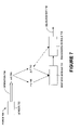
- FIG. 7 is a process view of measuring a force, according to one embodiment.
- FIG. 8 is a system view of a wheel connected to a moving device frame having a piston sensor device, according to one embodiment.
- FIG. 9 is a cross sectional view of the piston sensor device of FIG. 8 , according to one embodiment.
- FIG. 10 is a process flow to automatically generate a measurement based on an overlap area of a first conductive surface and a second conductive surface, according to one embodiment.
- An example embodiment provides methods and systems to automatically generate a measurement based on a change in an overlap area of a first conductive surface and a second conductive surface (e.g., the first conductive surface and the second conductive surface forming a sensor capacitor).
- the first conductive surface may be substantially parallel to the second conductive surface.
- the first conductive surface may be moveable relative to the second conductive surface in a direction substantially parallel with the second conductive surface.
- a reference capacitor may be used to adjust the measurement based on at least one environmental condition.
- the example embodiment may include communicating the measurement to a data processing system associated (e.g., through a wireless and/or a wired network) with the variable capacitor.
- the method may be in a form of a machine-readable medium embodying a set of instructions that, when executed by a machine, cause the machine to perform any method disclosed herein.
- Example embodiments of a method and a system, as described below, may be used to provide a high-accuracy, low-cost, load sensing devices (e.g., load sensors, pressure sensors, etc.). It will be appreciated that the various embodiments discussed herein may/may not be the same embodiment, and may be grouped into various other embodiments not explicitly disclosed herein.
- FIG. 1 is a device 150 formed by a top layer 102 (e.g., a conductive and/or non-conductive substrate) and a bottom layer 104 (e.g., a conductive and/or non-conductive substrate), according to one embodiment.
- a force 100 is applied to the top layer 102 in FIG. 1 .
- the top layer 102 includes a conductive surface 106 .
- the bottom layer 104 includes a conductive surface 108 and a conductive surface 110 .
- the conductive surface 106 and the conductive surface 108 (e.g., the conductive surface 106 and the conductive surface 108 may be substantially parallel to each other) form a sensor capacitor 114 (e.g., the sensor capacitor 114 may be a variable capacitor formed because two conductive surfaces/plates are separated and/or insulated from each other by an air dielectric between the conductive surface 106 and the conductive surface 108 ) in an area that overlaps the conductive surface 106 and the conductive surface 108 .
- the conductive surface 106 may be movable relative to the conductive surface 108 in one embodiment.
- a reference capacitor 112 is formed between the conductive surface 108 and the conductive surface 110 (e.g., a reference surface).
- the conductive surface 110 may be substantially parallel to the conductive surface 106 and/or with the conductive surface 108 in one embodiment.
- FIG. 2 is an assembly view of the device 150 , according to one embodiment.
- the top layer 102 and the bottom layer 104 are separated by a spacer 200 (e.g., a parameter spacer is illustrated; in other embodiments any type of spacer may be used).
- the spacer 200 may be used to physically separate the top layer 102 from the bottom layer 104 .
- the spacer 202 may be used to physically separate the bottom layer 104 from a bottom surface 204 .
- the spacers e.g., the spacer 200 and the spacer 202 ) may create gaps between various surfaces and layers. These gaps can be filled with air or any other gas (e.g., an inert gas).
- the bottom surface 204 may form an electromagnetic barrier for the device 150 and the outside environment (e.g., to protect against electromagnetic fields, etc.).
- the spacer 202 is at least ten times larger than the spacer 200 to account for stray capacitance between the bottom layer 104 and the bottom surface 204 .
- the spacer 202 and the bottom surface 204 are not required, and the bottom layer 104 is the lowest layer of the device 150 .
- FIG. 3 is a multi-depth device 350 according to one embodiment.
- a top layer 302 a middle layer 304 , and a bottom layer 314 are illustrated.
- the top layer 302 includes a conductive plate 306 (e.g., a conductive surface).
- the conductive plate 306 may be electrically separated from the top layer 302 by application of an insulating material between an area of affixation between the top layer 302 and the conductive plate 306 .
- a force 300 may be applied to the top layer 302 and the conductive plate 306 to cause the conductive plate 306 to deflect (e.g., move inward once a load and/or force 300 is applied to the top layer 302 as illustrated in FIG. 3 ).
- the middle layer 304 includes a conductive plate 308 and the conductive plate 310 .
- the middle layer 304 are two separate layers bonded together each having either the conductive plate 308 or the conductive plate 310 .
- the bottom layer 314 includes a conductive plate 316 .
- a shielding spacer (e.g., not shown, but the shielding spacer may be any type of spacer) between the reference capacitor (e.g., formed by the conductive plate 310 and the conductive plate 316 ) and a bottom of the housing (e.g., the bottom layer 314 ) to minimize an effect of a stray capacitance affecting the measurement (e.g., a height of the shielding spacer may be at least ten times larger than a plate spacer between plates of the reference capacitor and between plates of the sensor capacitor in one embodiment to minimize the stray capacitance).
- an area of each plate forming the reference capacitor e.g., the reference capacitor 112 of FIG.
- the conductive plate 306 and the conductive plate 308 may form a sensor capacitor (e.g., the sensor capacitor 114 as described in FIG. 1 ).
- the conductive plate 310 and the conductive plate 316 may form a reference capacitor (e.g., the reference capacitor 112 as described in FIG. 1 ).
- a spacer 311 may be used to physically separate the top layer 302 from the middle layer 304 .
- a spacer 312 may be used to physically separate the middle layer 304 from the bottom layer 314 .
- the multi-depth device 350 may be easier to manufacture according to one embodiment because of modularity of its design (e.g., various manufacturing techniques can be used to scale the multi-depth device 350 with a minimum number of sub-assemblies) in that various sub-assemblies may each include only one conductive surface (e.g., the top layer 302 , the middle layer 304 , and the bottom layer 316 may include only one conductive plate).
- FIG. 4 illustrates a bottom cup 414 (e.g., a housing) formed with a single block of material according to one embodiment.
- a single block e.g., steel
- the bottom cup 414 in FIG. 4 replaces the bottom layer 314 of FIG. 3 , and encompasses the various structures (e.g., capacitive surfaces/plates, spacers, etc.) between the bottom layer 314 and the top plate 302 as illustrated in FIG. 3 .
- the top layer 302 of FIG. 3 is a lid that fits on top of the bottom cup 414 .
- the bottom cup 414 may be formed from a single piece of metal through any process (e.g., involving cutting, milling, etching, drilling, etc.) that maintains the structural and/or tensile integrity of the bottom cup 414 . This way, the bottom cup 414 may be able to withstand larger amounts of force (e.g., the force 300 of FIG. 3 applied to a housing formed by the top layer 302 of FIG. 3 and the bottom cup 414 of FIG. 4 ) by channeling the force downward through the walls of the bottom cup 414 .
- any process e.g., involving cutting, milling, etching, drilling, etc.
- the bottom cup 414 may be able to withstand larger amounts of force (e.g., the force 300 of FIG. 3 applied to a housing formed by the top layer 302 of FIG. 3 and the bottom cup 414 of FIG. 4 ) by channeling the force downward through the walls of the bottom cup 414 .
- FIG. 5 illustrates a bottom cup 514 formed with multiple blocks of material according to one embodiment.
- multiple blocks e.g., of metal such as steel
- the bottom cup 514 in FIG. 5 replaces the bottom layer 314 of FIG. 3 , and encompasses the various structures (e.g., capacitive surfaces/plates, spacers, etc.) between the bottom layer 314 and the top plate 312 as illustrated in FIG. 3 .
- the top layer 302 of FIG. 3 is a lid that fits on top of the bottom cup 514 .
- the bottom cup 514 may be formed from multiple layers of metal that are each laser cut (e.g., laser etched) and/or patterned to form the bottom cup 514 at a cost lower than that of milling techniques in a single block.
- the layers 502 A– 502 N may be a standard metal size and/or shape, thereby reducing the cost of fabricating the bottom cup 514 .
- a single metal block may form a bottom layer 500 as illustrated in FIG. 5 . This way, the bottom cup 514 may be able to withstand larger amounts of force (e.g., the force 300 of FIG. 3 ) by channeling the force downward through the walls of the bottom cup 514 .
- FIG. 6 is a network enabled view of the device 150 of FIG. 1 , according to one embodiment.
- the first embodiment, a device 150 A is connected to a data processing system 602 through an interface cable 616 .
- the second device 150 B is wirelessly connected to the data processing system 602 through a network 600 .
- the network 600 is an Internet network.
- the network 600 is a local area network.
- a data processing system 606 may receive data (e.g., output data measuring force and/or load, etc.) from the device 150 A and/or the device 150 B through the network 600 .
- An access device 604 e.g., a device that enables wireless communication between devices forming a wireless network
- the device 150 B includes a transmitter/receiver circuit 608 and/or a wireless interface controller 610 for enabling the device 150 B to wirelessly communicate through the network 600 .
- the transmitter/receiver circuit 608 and/or the wireless interface controller 610 may be integrated in the processing module 714 of FIG. 7 .
- FIG. 7 is a process view of measuring a force 700 , according to one embodiment.
- a force 700 may be applied to a sensor 702 (e.g., the top layer 102 having the conductive surface 106 of FIG. 1 ), according to one embodiment.
- an electronic circuitry e.g., a software and/or hardware code
- a change in distance between the plates may be considered rather than a change in area.
- a change in capacitance 706 may be calculated based on the change in area overlapping two surfaces forming the sensor capacitor (e.g., as illustrated in FIG. 1 ).
- the change in capacitance 706 , a change in voltage 708 and/or a change in a frequency 710 may also be used to generate a measurement (e.g., an estimation of the force 700 applied to the sensor 702 ).
- the change in capacitance 706 data, the change in voltage 708 data, and/or the change in frequency data 710 may be provided to a digitizer module 712 (e.g., an analog-to-digital converter).
- the digitizer module 712 may work with the processing module 714 (e.g., a microprocessor integrated in the boxed device 350 of FIG. 3 ) to convert the change in capacitance 706 data, the change in voltage 708 data, and/or the change in frequency data 710 to a measurement reading (e.g., a measurement of the force 700 applied to the sensor 702 ).
- the processing module 714 is integrated in the device 150 of FIG. 1 , the boxed device 350 of FIG. 3 , and/or a piston sensor 850 of FIG. 8 .
- the processing module 714 may also detect the overlap area (e.g., the sensor capacitor 114 of FIG. 1 ) between the first conductive surface (e.g., the conductive surface 106 of FIG. 1 ) and the second conductive surface (e.g., the conductive surface 108 of FIG. 1 ), and may generate a measurement based on a position (e.g., amount of overlap) of the first conductive surface relative to the second conductive surface.
- the processing module may be configured to measure a reference capacitance between the reference surface and/or a selected surface (e.g., the conductive surface 106 and/or the conductive surface 108 ).
- FIG. 8 is a wheel 812 connected to a moving device frame 810 (e.g., the moving device frame may be an automobile, an airplane, a bicycle, etc.), according to one embodiment.
- the piston sensor device 850 is illustrated.
- the piston sensor 850 of FIG. 8 applies the various operations and principles illustrated in FIGS. 1–7 .
- the piston sensor 850 includes an inner conductive surface 800 , a middle conductive 802 , and an outer conductive surface 804 (e.g., may be coaxial to each other in that the inner conductive surface 800 , the middle conductive 802 , and/or the outer conductive surface 804 may share a common axis).
- the inner conductive surface 800 , the middle conductive 802 , and/or the outer conductive surface 804 have a substantially similar cross-sectional shape (e.g., a circle shape, a square shape, an ellipse shape, a rectangular shape, a rounded rectangle shape, a pentagon shape, a hexagon shape, and/or an octagon shape, etc.).
- the inner conductive surface 800 may be supported in the middle conductive surface 802 (e.g., a hollow tube) with a spacer 806 A and a spacer 806 B (e.g., the spacers may be made of Teflon).
- the top of the piston sensor 850 may be physically coupled to the moving device frame 810 , so as the middle conductive surface 802 and the outer conductive surface 804 do not move.
- the inner conductive surface 800 may move with motion of the moving device (e.g., a car) and with rotation of the wheel 812 .
- FIG. 9 is a cross sectional view 808 (e.g., as illustrated in FIG. 8 ) of the piston sensor 850 , according to one embodiment.
- the inner conductive surface 800 of FIG. 8 is illustrated as a filled metal tube (e.g. in alternate embodiments may not be a filled metal tube).
- the middle conductive surface 802 is illustrates a hollow conductive tube.
- a spacer e.g.
- the spacer 806 A and/or the spacer 806 B may hold the inner conductive surface 800 inside the middle conductive surface 802 .
- the inner conductive surface 800 and the middle conductive surface 802 may be separated by a gap 900 .
- a sensor capacitor may be formed (e.g., the sensor capacitor 114 as described in FIG. 1 ).
- the capacitance of the sensor capacitor may change (e.g., the change in capacitance 706 of FIG. 7 ).
- the outer conductive surface 804 and the middle conductive surface 802 as illustrated in FIG. 9 may form the reference capacitor (e.g., the reference capacitor 112 of FIG. 1 ).
- a gap 902 e.g., an air gap forming a gap between two metal plates and/or between metallic tubes
- the capacitance between these two surfaces does not change because of the motion of the wheel 812 of FIG. 8 (e.g., the relative capacitance between the middle conductive surface 802 and the outer conductive surface 804 is not affected by the motion of the wheel 812 ).
- FIG. 10 is a process flow to automatically generate (e.g., using the processing module 714 as illustrated in FIG. 7 ) a measurement based on an overlap area (e.g., the overlap area illustrated by the sensor capacitor 114 in FIG. 1 ) of a first conductive surface and a second conductive surface, according to one embodiment.
- a first conductive surface e.g., the conductive surface 106 of FIG. 1
- second conductive surface e.g., the conductive surface 108 of FIG. 1
- non-conductive printed circuit boards e.g., the top layer 102 and the bottom layer 104 respectively.
- a sensor capacitor e.g., the sensor capacitor 114 of FIG. 1
- a reference capacitor e.g., the reference capacitor 112 of FIG. 1
- a measurement is automatically generated based on a change in an overlap area of the first conductive surface (e.g., the conductive surface 106 of FIG. 1 ) and the second conductive surface (e.g., the conductive surface 108 of FIG. 1 ).
- the area of overlap may change when the force 100 of FIG.
- the change in the area is caused by a deflection of the first conductive surface (e.g., the conductive surface 108 may deflect when the force 100 of FIG. 1 is applied) with respect to the second conductive surface.
- an algorithm e.g., an iterative algorithm
- the measurement is adjusted based on at least one environmental condition by analyzing data of the reference capacitor (e.g., the environmental condition may be humidity in a gap between the first conductive surface and the second conductive surface, a temperature of the apparatus, and/or an air pressure of an environment surrounding the apparatus, etc.).
- the measurement may be communicated to a data processing system (e.g., the data processing system 602 as illustrated in FIG. 6 ) associated (e.g., either through the cable 616 and/or through the network 600 of FIG. 6 ) with the variable capacitor (e.g., the sensor device 114 in the device 150 of FIG. 1 ) in operation 1012 .
- a data processing system e.g., the data processing system 602 as illustrated in FIG. 6
- the variable capacitor e.g., the sensor device 114 in the device 150 of FIG. 1
- the transmitter/receiver circuit 608 of FIG. 6 , the wireless interface controller 610 of FIG. 6 , and/or the processing module 714 of FIG. 7 described herein may be enabled and operated using hardware circuitry (e.g., CMOS based logic circuitry), firmware, software and/or any combination of hardware, firmware, and/or software (e.g., embodied in a machine readable medium).
- hardware circuitry e.g., CMOS based logic circuitry
- firmware software and/or any combination of hardware, firmware, and/or software (e.g., embodied in a machine readable medium).
- the digital converter module 712 and/or the processing module 714 may be enabled using software and/or using transistors, logic gates, and electrical circuits (e.g., application specific integrated ASIC circuitry) such as a digital converter circuit and/or a processing circuit.
- electrical circuits e.g., application specific integrated ASIC circuitry
- the various operations, processes, and methods disclosed herein may be embodied in a machine-readable medium and/or a machine accessible medium compatible with a data processing system (e.g., a computer system), and may be performed in any order (e.g., including using means for achieving the various operations). Accordingly, the specification and drawings are to be regarded in an illustrative rather than a restrictive sense.
Abstract
Description
Claims (21)
Priority Applications (4)
| Application Number | Priority Date | Filing Date | Title |
|---|---|---|---|
| US11/237,353 US7187185B2 (en) | 2004-09-29 | 2005-09-28 | Area-change sensing through capacitive techniques |
| US12/032,718 US7921728B2 (en) | 2003-04-09 | 2008-02-18 | Flexible apparatus and method to enhance capacitive force sensing |
| US12/487,696 US20090259413A1 (en) | 2003-04-09 | 2009-06-19 | Resistive force sensing device and method with an advanced communication interface |
| US12/615,275 US20100076701A1 (en) | 2004-04-09 | 2009-11-10 | Resistive force sensing device and method with an advanced communication interface |
Applications Claiming Priority (2)
| Application Number | Priority Date | Filing Date | Title |
|---|---|---|---|
| US61423604P | 2004-09-29 | 2004-09-29 | |
| US11/237,353 US7187185B2 (en) | 2004-09-29 | 2005-09-28 | Area-change sensing through capacitive techniques |
Related Parent Applications (3)
| Application Number | Title | Priority Date | Filing Date |
|---|---|---|---|
| US11/237,060 Continuation-In-Part US7451659B2 (en) | 2003-04-09 | 2005-09-28 | Gap-change sensing through capacitive techniques |
| US11/305,673 Continuation US7353713B2 (en) | 2003-04-09 | 2005-12-16 | Flexible apparatus and method to enhance capacitive force sensing |
| US11/305,673 Continuation-In-Part US7353713B2 (en) | 2003-04-09 | 2005-12-16 | Flexible apparatus and method to enhance capacitive force sensing |
Related Child Applications (3)
| Application Number | Title | Priority Date | Filing Date |
|---|---|---|---|
| US11/237,060 Continuation US7451659B2 (en) | 2003-04-09 | 2005-09-28 | Gap-change sensing through capacitive techniques |
| US11/237,060 Continuation-In-Part US7451659B2 (en) | 2003-04-09 | 2005-09-28 | Gap-change sensing through capacitive techniques |
| US11/305,673 Continuation-In-Part US7353713B2 (en) | 2003-04-09 | 2005-12-16 | Flexible apparatus and method to enhance capacitive force sensing |
Publications (2)
| Publication Number | Publication Date |
|---|---|
| US20060066319A1 US20060066319A1 (en) | 2006-03-30 |
| US7187185B2 true US7187185B2 (en) | 2007-03-06 |
Family
ID=36098299
Family Applications (1)
| Application Number | Title | Priority Date | Filing Date |
|---|---|---|---|
| US11/237,353 Active US7187185B2 (en) | 2003-04-09 | 2005-09-28 | Area-change sensing through capacitive techniques |
Country Status (1)
| Country | Link |
|---|---|
| US (1) | US7187185B2 (en) |
Cited By (8)
| Publication number | Priority date | Publication date | Assignee | Title |
|---|---|---|---|---|
| CN1034441C (en) * | 1993-08-12 | 1997-04-02 | 武汉大学 | Time identifying electrochemistry quartz crystal micro-balance |
| US7343814B2 (en) * | 2006-04-03 | 2008-03-18 | Loadstar Sensors, Inc. | Multi-zone capacitive force sensing device and methods |
| US7451659B2 (en) * | 2004-09-29 | 2008-11-18 | Loadstar Sensors, Inc. | Gap-change sensing through capacitive techniques |
| US20090120198A1 (en) * | 2005-09-28 | 2009-05-14 | Dallenbach William D | Gap-change sensing through capacitive techniques |
| US20090160460A1 (en) * | 2007-12-23 | 2009-06-25 | Divyasimha Harish | Analysis of a material with capacitive technology |
| US20090206098A1 (en) * | 2008-02-19 | 2009-08-20 | Garahan Patrick J | Portable holder for beverage containers |
| US7737514B1 (en) | 2008-02-21 | 2010-06-15 | Yee-Chung Fu | MEMS pressure sensor using area-change capacitive technique |
| US8334159B1 (en) | 2009-03-30 | 2012-12-18 | Advanced Numicro Systems, Inc. | MEMS pressure sensor using capacitive technique |
Families Citing this family (57)
| Publication number | Priority date | Publication date | Assignee | Title |
|---|---|---|---|---|
| US7443174B2 (en) * | 2006-04-06 | 2008-10-28 | Freescale Semiconductor, Inc. | Electric field reciprocal displacement sensors |
| JP2008196933A (en) * | 2007-02-13 | 2008-08-28 | Nitta Ind Corp | Force measuring device |
| US7673530B2 (en) * | 2007-03-20 | 2010-03-09 | Loadstar Sensors, Inc. | Capacitive sensor based structure and method with tilt compensation capability |
| US7980145B2 (en) * | 2007-12-27 | 2011-07-19 | Y Point Capital, Inc | Microelectromechanical capacitive device |
| US20110180781A1 (en) * | 2008-06-05 | 2011-07-28 | Soraa, Inc | Highly Polarized White Light Source By Combining Blue LED on Semipolar or Nonpolar GaN with Yellow LED on Semipolar or Nonpolar GaN |
| US20090309127A1 (en) * | 2008-06-13 | 2009-12-17 | Soraa, Inc. | Selective area epitaxy growth method and structure |
| US8847249B2 (en) * | 2008-06-16 | 2014-09-30 | Soraa, Inc. | Solid-state optical device having enhanced indium content in active regions |
| US20100006873A1 (en) * | 2008-06-25 | 2010-01-14 | Soraa, Inc. | HIGHLY POLARIZED WHITE LIGHT SOURCE BY COMBINING BLUE LED ON SEMIPOLAR OR NONPOLAR GaN WITH YELLOW LED ON SEMIPOLAR OR NONPOLAR GaN |
| US8259769B1 (en) | 2008-07-14 | 2012-09-04 | Soraa, Inc. | Integrated total internal reflectors for high-gain laser diodes with high quality cleaved facets on nonpolar/semipolar GaN substrates |
| US8805134B1 (en) | 2012-02-17 | 2014-08-12 | Soraa Laser Diode, Inc. | Methods and apparatus for photonic integration in non-polar and semi-polar oriented wave-guided optical devices |
| US8384399B2 (en) * | 2008-08-28 | 2013-02-26 | Infineon Technologies Ag | System including capacitively coupled electrodes and circuits in a network |
| US8436816B2 (en) * | 2008-10-24 | 2013-05-07 | Apple Inc. | Disappearing button or slider |
| JP5780605B2 (en) * | 2009-04-13 | 2015-09-16 | ソラア レイザー ダイオード インク | Optical element structure using GAN substrate for laser utilization |
| US8634442B1 (en) | 2009-04-13 | 2014-01-21 | Soraa Laser Diode, Inc. | Optical device structure using GaN substrates for laser applications |
| US8837545B2 (en) | 2009-04-13 | 2014-09-16 | Soraa Laser Diode, Inc. | Optical device structure using GaN substrates and growth structures for laser applications |
| US9829780B2 (en) | 2009-05-29 | 2017-11-28 | Soraa Laser Diode, Inc. | Laser light source for a vehicle |
| US8509275B1 (en) | 2009-05-29 | 2013-08-13 | Soraa, Inc. | Gallium nitride based laser dazzling device and method |
| US9800017B1 (en) | 2009-05-29 | 2017-10-24 | Soraa Laser Diode, Inc. | Laser device and method for a vehicle |
| US8427590B2 (en) | 2009-05-29 | 2013-04-23 | Soraa, Inc. | Laser based display method and system |
| US10108079B2 (en) | 2009-05-29 | 2018-10-23 | Soraa Laser Diode, Inc. | Laser light source for a vehicle |
| US9250044B1 (en) | 2009-05-29 | 2016-02-02 | Soraa Laser Diode, Inc. | Gallium and nitrogen containing laser diode dazzling devices and methods of use |
| US8750342B1 (en) | 2011-09-09 | 2014-06-10 | Soraa Laser Diode, Inc. | Laser diodes with scribe structures |
| US8355418B2 (en) | 2009-09-17 | 2013-01-15 | Soraa, Inc. | Growth structures and method for forming laser diodes on {20-21} or off cut gallium and nitrogen containing substrates |
| US9927611B2 (en) | 2010-03-29 | 2018-03-27 | Soraa Laser Diode, Inc. | Wearable laser based display method and system |
| US20110242041A1 (en) * | 2010-04-01 | 2011-10-06 | Nokia Corporation | Method and Apparatus for Performing a Function |
| US8816319B1 (en) | 2010-11-05 | 2014-08-26 | Soraa Laser Diode, Inc. | Method of strain engineering and related optical device using a gallium and nitrogen containing active region |
| US9318875B1 (en) | 2011-01-24 | 2016-04-19 | Soraa Laser Diode, Inc. | Color converting element for laser diode |
| US9025635B2 (en) | 2011-01-24 | 2015-05-05 | Soraa Laser Diode, Inc. | Laser package having multiple emitters configured on a support member |
| US9595813B2 (en) | 2011-01-24 | 2017-03-14 | Soraa Laser Diode, Inc. | Laser package having multiple emitters configured on a substrate member |
| US9093820B1 (en) | 2011-01-25 | 2015-07-28 | Soraa Laser Diode, Inc. | Method and structure for laser devices using optical blocking regions |
| US9236530B2 (en) | 2011-04-01 | 2016-01-12 | Soraa, Inc. | Miscut bulk substrates |
| US9646827B1 (en) | 2011-08-23 | 2017-05-09 | Soraa, Inc. | Method for smoothing surface of a substrate containing gallium and nitrogen |
| US9166372B1 (en) | 2013-06-28 | 2015-10-20 | Soraa Laser Diode, Inc. | Gallium nitride containing laser device configured on a patterned substrate |
| US9368939B2 (en) | 2013-10-18 | 2016-06-14 | Soraa Laser Diode, Inc. | Manufacturable laser diode formed on C-plane gallium and nitrogen material |
| US9520695B2 (en) | 2013-10-18 | 2016-12-13 | Soraa Laser Diode, Inc. | Gallium and nitrogen containing laser device having confinement region |
| US9379525B2 (en) | 2014-02-10 | 2016-06-28 | Soraa Laser Diode, Inc. | Manufacturable laser diode |
| US9362715B2 (en) | 2014-02-10 | 2016-06-07 | Soraa Laser Diode, Inc | Method for manufacturing gallium and nitrogen bearing laser devices with improved usage of substrate material |
| US9209596B1 (en) | 2014-02-07 | 2015-12-08 | Soraa Laser Diode, Inc. | Manufacturing a laser diode device from a plurality of gallium and nitrogen containing substrates |
| US9520697B2 (en) | 2014-02-10 | 2016-12-13 | Soraa Laser Diode, Inc. | Manufacturable multi-emitter laser diode |
| US9871350B2 (en) | 2014-02-10 | 2018-01-16 | Soraa Laser Diode, Inc. | Manufacturable RGB laser diode source |
| US9564736B1 (en) * | 2014-06-26 | 2017-02-07 | Soraa Laser Diode, Inc. | Epitaxial growth of p-type cladding regions using nitrogen gas for a gallium and nitrogen containing laser diode |
| US9246311B1 (en) | 2014-11-06 | 2016-01-26 | Soraa Laser Diode, Inc. | Method of manufacture for an ultraviolet laser diode |
| US9666677B1 (en) | 2014-12-23 | 2017-05-30 | Soraa Laser Diode, Inc. | Manufacturable thin film gallium and nitrogen containing devices |
| US9653642B1 (en) | 2014-12-23 | 2017-05-16 | Soraa Laser Diode, Inc. | Manufacturable RGB display based on thin film gallium and nitrogen containing light emitting diodes |
| US10879673B2 (en) | 2015-08-19 | 2020-12-29 | Soraa Laser Diode, Inc. | Integrated white light source using a laser diode and a phosphor in a surface mount device package |
| US10938182B2 (en) | 2015-08-19 | 2021-03-02 | Soraa Laser Diode, Inc. | Specialized integrated light source using a laser diode |
| US11437775B2 (en) | 2015-08-19 | 2022-09-06 | Kyocera Sld Laser, Inc. | Integrated light source using a laser diode |
| US11437774B2 (en) | 2015-08-19 | 2022-09-06 | Kyocera Sld Laser, Inc. | High-luminous flux laser-based white light source |
| US9787963B2 (en) | 2015-10-08 | 2017-10-10 | Soraa Laser Diode, Inc. | Laser lighting having selective resolution |
| US10771155B2 (en) | 2017-09-28 | 2020-09-08 | Soraa Laser Diode, Inc. | Intelligent visible light with a gallium and nitrogen containing laser source |
| US10222474B1 (en) | 2017-12-13 | 2019-03-05 | Soraa Laser Diode, Inc. | Lidar systems including a gallium and nitrogen containing laser light source |
| US10551728B1 (en) | 2018-04-10 | 2020-02-04 | Soraa Laser Diode, Inc. | Structured phosphors for dynamic lighting |
| US11239637B2 (en) | 2018-12-21 | 2022-02-01 | Kyocera Sld Laser, Inc. | Fiber delivered laser induced white light system |
| US11421843B2 (en) | 2018-12-21 | 2022-08-23 | Kyocera Sld Laser, Inc. | Fiber-delivered laser-induced dynamic light system |
| US11884202B2 (en) | 2019-01-18 | 2024-01-30 | Kyocera Sld Laser, Inc. | Laser-based fiber-coupled white light system |
| US10903623B2 (en) | 2019-05-14 | 2021-01-26 | Soraa Laser Diode, Inc. | Method and structure for manufacturable large area gallium and nitrogen containing substrate |
| US11228158B2 (en) | 2019-05-14 | 2022-01-18 | Kyocera Sld Laser, Inc. | Manufacturable laser diodes on a large area gallium and nitrogen containing substrate |
Citations (17)
| Publication number | Priority date | Publication date | Assignee | Title |
|---|---|---|---|---|
| US3928796A (en) * | 1973-11-30 | 1975-12-23 | Int Lead Zinc Res | Capacitive displacement transducer |
| US4961055A (en) * | 1989-01-04 | 1990-10-02 | Vickers, Incorporated | Linear capacitance displacement transducer |
| US5068796A (en) * | 1989-12-18 | 1991-11-26 | E. I. Du Pont De Nemours And Company | Control of sheet opacity |
| US5774048A (en) * | 1993-02-08 | 1998-06-30 | Alpha-Beta Electronics Ag | Valve having means for generating a wireless transmittable indicating signal in case of a pressure drop within vehicle tires |
| US6026694A (en) | 1998-03-30 | 2000-02-22 | Serena Industries Incorporated | Linear force sensing device |
| US6079282A (en) | 1998-06-26 | 2000-06-27 | Bossard Technologies Ag | Capacitive force sensor |
| US20020063688A1 (en) | 1999-11-04 | 2002-05-30 | Synaptics Incorporated | Capacitive mouse |
| US20020191029A1 (en) | 2001-05-16 | 2002-12-19 | Synaptics, Inc. | Touch screen with user interface enhancement |
| US20030062889A1 (en) | 1996-12-12 | 2003-04-03 | Synaptics (Uk) Limited | Position detector |
| US20030160808A1 (en) | 2001-06-07 | 2003-08-28 | Synaptics, Inc. | Method and apparatus for controlling a display of data on a display screen |
| US20040178997A1 (en) | 1992-06-08 | 2004-09-16 | Synaptics, Inc., A California Corporation | Object position detector with edge motion feature and gesture recognition |
| US20040252109A1 (en) | 2002-04-11 | 2004-12-16 | Synaptics, Inc. | Closed-loop sensor on a solid-state object position detector |
| US20050021269A1 (en) | 2003-07-24 | 2005-01-27 | Synaptics (Uk) Limited | Magnetic calibration array |
| US20050024341A1 (en) | 2001-05-16 | 2005-02-03 | Synaptics, Inc. | Touch screen with user interface enhancement |
| US20050148884A1 (en) * | 2003-10-10 | 2005-07-07 | Parks Thomas R. | High resolution solid state pressure sensor |
| US20050171714A1 (en) | 2002-03-05 | 2005-08-04 | Synaptics (Uk) Limited | Position sensor |
| US20050168489A1 (en) | 2004-01-29 | 2005-08-04 | Synaptics Incorporated | Method and apparatus for producing one-dimensional signals with a two-dimensional pointing device |
-
2005
- 2005-09-28 US US11/237,353 patent/US7187185B2/en active Active
Patent Citations (20)
| Publication number | Priority date | Publication date | Assignee | Title |
|---|---|---|---|---|
| US3928796A (en) * | 1973-11-30 | 1975-12-23 | Int Lead Zinc Res | Capacitive displacement transducer |
| US4961055A (en) * | 1989-01-04 | 1990-10-02 | Vickers, Incorporated | Linear capacitance displacement transducer |
| US5068796A (en) * | 1989-12-18 | 1991-11-26 | E. I. Du Pont De Nemours And Company | Control of sheet opacity |
| US20040178997A1 (en) | 1992-06-08 | 2004-09-16 | Synaptics, Inc., A California Corporation | Object position detector with edge motion feature and gesture recognition |
| US5774048A (en) * | 1993-02-08 | 1998-06-30 | Alpha-Beta Electronics Ag | Valve having means for generating a wireless transmittable indicating signal in case of a pressure drop within vehicle tires |
| US20040169594A1 (en) | 1994-05-14 | 2004-09-02 | Synaptics (Uk) Limited | Position detector |
| US20030062889A1 (en) | 1996-12-12 | 2003-04-03 | Synaptics (Uk) Limited | Position detector |
| US6026694A (en) | 1998-03-30 | 2000-02-22 | Serena Industries Incorporated | Linear force sensing device |
| US6079282A (en) | 1998-06-26 | 2000-06-27 | Bossard Technologies Ag | Capacitive force sensor |
| US20020063688A1 (en) | 1999-11-04 | 2002-05-30 | Synaptics Incorporated | Capacitive mouse |
| US20030156098A1 (en) | 1999-11-04 | 2003-08-21 | Synaptics, Inc. | Capacitive mouse |
| US20050024341A1 (en) | 2001-05-16 | 2005-02-03 | Synaptics, Inc. | Touch screen with user interface enhancement |
| US20020191029A1 (en) | 2001-05-16 | 2002-12-19 | Synaptics, Inc. | Touch screen with user interface enhancement |
| US20030160808A1 (en) | 2001-06-07 | 2003-08-28 | Synaptics, Inc. | Method and apparatus for controlling a display of data on a display screen |
| US20050171714A1 (en) | 2002-03-05 | 2005-08-04 | Synaptics (Uk) Limited | Position sensor |
| US20040252109A1 (en) | 2002-04-11 | 2004-12-16 | Synaptics, Inc. | Closed-loop sensor on a solid-state object position detector |
| US20050156881A1 (en) | 2002-04-11 | 2005-07-21 | Synaptics, Inc. | Closed-loop sensor on a solid-state object position detector |
| US20050021269A1 (en) | 2003-07-24 | 2005-01-27 | Synaptics (Uk) Limited | Magnetic calibration array |
| US20050148884A1 (en) * | 2003-10-10 | 2005-07-07 | Parks Thomas R. | High resolution solid state pressure sensor |
| US20050168489A1 (en) | 2004-01-29 | 2005-08-04 | Synaptics Incorporated | Method and apparatus for producing one-dimensional signals with a two-dimensional pointing device |
Non-Patent Citations (2)
| Title |
|---|
| "Model MCL Internally Amplified Miniature Tension/Compression Load Cell", http://www.rdpelectrosense.com/load/mcl.htm, 3 pages. |
| "Weighing Systems: Scales, Balances and Load Cells:Setra", Setra Weighing Systems Division; http://www.setra.com/wei/index.htm, 2 Pages. |
Cited By (10)
| Publication number | Priority date | Publication date | Assignee | Title |
|---|---|---|---|---|
| CN1034441C (en) * | 1993-08-12 | 1997-04-02 | 武汉大学 | Time identifying electrochemistry quartz crystal micro-balance |
| US7451659B2 (en) * | 2004-09-29 | 2008-11-18 | Loadstar Sensors, Inc. | Gap-change sensing through capacitive techniques |
| US20090120198A1 (en) * | 2005-09-28 | 2009-05-14 | Dallenbach William D | Gap-change sensing through capacitive techniques |
| US7343814B2 (en) * | 2006-04-03 | 2008-03-18 | Loadstar Sensors, Inc. | Multi-zone capacitive force sensing device and methods |
| US20090160460A1 (en) * | 2007-12-23 | 2009-06-25 | Divyasimha Harish | Analysis of a material with capacitive technology |
| US8174272B2 (en) * | 2007-12-23 | 2012-05-08 | Ypoint Capital, Inc. | Analysis of a material with capacitive technology |
| US20090206098A1 (en) * | 2008-02-19 | 2009-08-20 | Garahan Patrick J | Portable holder for beverage containers |
| US8066148B2 (en) | 2008-02-19 | 2011-11-29 | Garahan Patrick J | Portable holder for beverage containers |
| US7737514B1 (en) | 2008-02-21 | 2010-06-15 | Yee-Chung Fu | MEMS pressure sensor using area-change capacitive technique |
| US8334159B1 (en) | 2009-03-30 | 2012-12-18 | Advanced Numicro Systems, Inc. | MEMS pressure sensor using capacitive technique |
Also Published As
| Publication number | Publication date |
|---|---|
| US20060066319A1 (en) | 2006-03-30 |
Similar Documents
| Publication | Publication Date | Title |
|---|---|---|
| US7187185B2 (en) | Area-change sensing through capacitive techniques | |
| US7451659B2 (en) | Gap-change sensing through capacitive techniques | |
| US7353713B2 (en) | Flexible apparatus and method to enhance capacitive force sensing | |
| CN1864054B (en) | Capacitive sensor | |
| EP1728058B1 (en) | Load cell including displacement transducer, and associated methods of use and manufacture | |
| Huang et al. | A flexible three-axial capacitive tactile sensor with multilayered dielectric for artificial skin applications | |
| US20030015043A1 (en) | Force detector and acceleration detector and method of manufacturing the same | |
| US20090158856A1 (en) | Capacitive strain gauge system and method | |
| KR20050044732A (en) | Sealed load cell | |
| CN101982864B (en) | Movable electrode of variable capacitor, pressure sensor and blood pressure measuring equipment | |
| US7921728B2 (en) | Flexible apparatus and method to enhance capacitive force sensing | |
| CN107976274B (en) | Pressure detection device and method based on synchronous resonance | |
| US20090120198A1 (en) | Gap-change sensing through capacitive techniques | |
| US7690270B1 (en) | Load measuring transducer using induced voltage for overcoming eccentric errors and load measuring system using the same | |
| Das et al. | Simple approach to design a capacitive rotary encoder | |
| Qiulin et al. | High temperature characteristic for wireless pressure LTCC-based sensor | |
| CN104990663B (en) | Contact type parallel plate differential three-dimensional force pressure sensor | |
| CN204675826U (en) | MEMS pressure sensor, MEMS inertial sensor integrated morphology | |
| Kisić et al. | Performance analysis of a flexible polyimide based device for displacement sensing | |
| US6633172B1 (en) | Capacitive measuring sensor and method for operating same | |
| US20190095024A1 (en) | Pressure sensing device and electronic apparatus having same | |
| US8082804B2 (en) | Load measuring transducer using induced voltage for reducing measuring errors and load measuring system using the same | |
| CN116940818A (en) | Device for measuring deformations, stresses, forces and/or torques in a plurality of shafts | |
| JPH085482A (en) | Electrostatic capacity type tactile sensor | |
| Ferrari et al. | Printed thick-film capacitive sensors |
Legal Events
| Date | Code | Title | Description |
|---|---|---|---|
| AS | Assignment |
Owner name: LOADSTAR SENSORS, INC., CALIFORNIA Free format text: ASSIGNMENT OF ASSIGNORS INTEREST;ASSIGNORS:DALLENBACH, WILLIAM D.;HARISH, DIVYASIMHA;REEL/FRAME:017071/0419 Effective date: 20050928 |
|
| AS | Assignment |
Owner name: SILICON VALLEY BANK, CALIFORNIA Free format text: SECURITY AGREEMENT;ASSIGNOR:LOADSTAR SENSORS INC.;REEL/FRAME:018415/0023 Effective date: 20060621 |
|
| AS | Assignment |
Owner name: LOADSTAR SENSORS, INC., CALIFORNIA Free format text: RELEASE;ASSIGNOR:SILICON VALLEY BANK;REEL/FRAME:018778/0834 Effective date: 20061221 |
|
| STCF | Information on status: patent grant |
Free format text: PATENTED CASE |
|
| CC | Certificate of correction | ||
| CC | Certificate of correction | ||
| FPAY | Fee payment |
Year of fee payment: 4 |
|
| AS | Assignment |
Owner name: YPOINT CAPITAL, INC,, CALIFORNIA Free format text: ASSIGNMENT OF ASSIGNORS INTEREST;ASSIGNOR:LOADSTAR SENSORS, INC.;REEL/FRAME:025622/0842 Effective date: 20101229 |
|
| REMI | Maintenance fee reminder mailed | ||
| FPAY | Fee payment |
Year of fee payment: 8 |
|
| SULP | Surcharge for late payment |
Year of fee payment: 7 |
|
| MAFP | Maintenance fee payment |
Free format text: PAYMENT OF MAINTENANCE FEE, 12TH YR, SMALL ENTITY (ORIGINAL EVENT CODE: M2553); ENTITY STATUS OF PATENT OWNER: SMALL ENTITY Year of fee payment: 12 |