US9564473B2 - Display device - Google Patents
Display device Download PDFInfo
- Publication number
- US9564473B2 US9564473B2 US14/819,962 US201514819962A US9564473B2 US 9564473 B2 US9564473 B2 US 9564473B2 US 201514819962 A US201514819962 A US 201514819962A US 9564473 B2 US9564473 B2 US 9564473B2
- Authority
- US
- United States
- Prior art keywords
- layer
- display
- display panel
- light
- substrate
- Prior art date
- Legal status (The legal status is an assumption and is not a legal conclusion. Google has not performed a legal analysis and makes no representation as to the accuracy of the status listed.)
- Active
Links
- 230000003287 optical effect Effects 0.000 claims description 5
- 239000010410 layer Substances 0.000 description 413
- 239000000758 substrate Substances 0.000 description 127
- 229920005989 resin Polymers 0.000 description 61
- 239000011347 resin Substances 0.000 description 61
- 239000000463 material Substances 0.000 description 45
- 238000000926 separation method Methods 0.000 description 41
- 238000000034 method Methods 0.000 description 36
- 230000015572 biosynthetic process Effects 0.000 description 34
- 239000004065 semiconductor Substances 0.000 description 26
- 238000007789 sealing Methods 0.000 description 24
- 238000004040 coloring Methods 0.000 description 21
- 239000000956 alloy Substances 0.000 description 19
- WFKWXMTUELFFGS-UHFFFAOYSA-N tungsten Chemical compound [W] WFKWXMTUELFFGS-UHFFFAOYSA-N 0.000 description 19
- 229910052721 tungsten Inorganic materials 0.000 description 19
- 239000010937 tungsten Substances 0.000 description 19
- 239000007769 metal material Substances 0.000 description 18
- XLYOFNOQVPJJNP-UHFFFAOYSA-N water Substances O XLYOFNOQVPJJNP-UHFFFAOYSA-N 0.000 description 17
- PXHVJJICTQNCMI-UHFFFAOYSA-N Nickel Chemical compound [Ni] PXHVJJICTQNCMI-UHFFFAOYSA-N 0.000 description 16
- 239000011521 glass Substances 0.000 description 15
- 238000004519 manufacturing process Methods 0.000 description 14
- 229910044991 metal oxide Inorganic materials 0.000 description 14
- 150000004706 metal oxides Chemical class 0.000 description 14
- 239000002245 particle Substances 0.000 description 13
- 230000035699 permeability Effects 0.000 description 13
- ZOKXTWBITQBERF-UHFFFAOYSA-N Molybdenum Chemical compound [Mo] ZOKXTWBITQBERF-UHFFFAOYSA-N 0.000 description 11
- 229910045601 alloy Inorganic materials 0.000 description 11
- 238000000605 extraction Methods 0.000 description 11
- 239000012535 impurity Substances 0.000 description 11
- 229910052751 metal Inorganic materials 0.000 description 11
- 239000002184 metal Substances 0.000 description 11
- 239000011733 molybdenum Substances 0.000 description 11
- XLOMVQKBTHCTTD-UHFFFAOYSA-N Zinc monoxide Chemical compound [Zn]=O XLOMVQKBTHCTTD-UHFFFAOYSA-N 0.000 description 10
- 229910052750 molybdenum Inorganic materials 0.000 description 10
- 239000000126 substance Substances 0.000 description 10
- IJGRMHOSHXDMSA-UHFFFAOYSA-N Atomic nitrogen Chemical compound N#N IJGRMHOSHXDMSA-UHFFFAOYSA-N 0.000 description 9
- 229910052782 aluminium Inorganic materials 0.000 description 9
- XAGFODPZIPBFFR-UHFFFAOYSA-N aluminium Chemical compound [Al] XAGFODPZIPBFFR-UHFFFAOYSA-N 0.000 description 9
- 239000011810 insulating material Substances 0.000 description 9
- KDLHZDBZIXYQEI-UHFFFAOYSA-N Palladium Chemical compound [Pd] KDLHZDBZIXYQEI-UHFFFAOYSA-N 0.000 description 8
- VYPSYNLAJGMNEJ-UHFFFAOYSA-N Silicium dioxide Chemical compound O=[Si]=O VYPSYNLAJGMNEJ-UHFFFAOYSA-N 0.000 description 8
- XUIMIQQOPSSXEZ-UHFFFAOYSA-N Silicon Chemical compound [Si] XUIMIQQOPSSXEZ-UHFFFAOYSA-N 0.000 description 8
- QVQLCTNNEUAWMS-UHFFFAOYSA-N barium oxide Chemical compound [Ba]=O QVQLCTNNEUAWMS-UHFFFAOYSA-N 0.000 description 8
- 229910052759 nickel Inorganic materials 0.000 description 8
- 229910052710 silicon Inorganic materials 0.000 description 8
- 239000010703 silicon Substances 0.000 description 8
- RYGMFSIKBFXOCR-UHFFFAOYSA-N Copper Chemical compound [Cu] RYGMFSIKBFXOCR-UHFFFAOYSA-N 0.000 description 7
- 229910052581 Si3N4 Inorganic materials 0.000 description 7
- RTAQQCXQSZGOHL-UHFFFAOYSA-N Titanium Chemical compound [Ti] RTAQQCXQSZGOHL-UHFFFAOYSA-N 0.000 description 7
- QVGXLLKOCUKJST-UHFFFAOYSA-N atomic oxygen Chemical compound [O] QVGXLLKOCUKJST-UHFFFAOYSA-N 0.000 description 7
- 239000010949 copper Substances 0.000 description 7
- 230000000994 depressogenic effect Effects 0.000 description 7
- 238000005530 etching Methods 0.000 description 7
- 229910052760 oxygen Inorganic materials 0.000 description 7
- 239000001301 oxygen Substances 0.000 description 7
- HQVNEWCFYHHQES-UHFFFAOYSA-N silicon nitride Chemical compound N12[Si]34N5[Si]62N3[Si]51N64 HQVNEWCFYHHQES-UHFFFAOYSA-N 0.000 description 7
- 229910052719 titanium Inorganic materials 0.000 description 7
- 239000010936 titanium Substances 0.000 description 7
- 229910001316 Ag alloy Inorganic materials 0.000 description 6
- GQPLMRYTRLFLPF-UHFFFAOYSA-N Nitrous Oxide Chemical compound [O-][N+]#N GQPLMRYTRLFLPF-UHFFFAOYSA-N 0.000 description 6
- 239000007789 gas Substances 0.000 description 6
- 239000000203 mixture Substances 0.000 description 6
- -1 polyethylene terephthalate Polymers 0.000 description 6
- 229920001721 polyimide Polymers 0.000 description 6
- 238000007639 printing Methods 0.000 description 6
- 239000004925 Acrylic resin Substances 0.000 description 5
- 229920000178 Acrylic resin Polymers 0.000 description 5
- BQCADISMDOOEFD-UHFFFAOYSA-N Silver Chemical compound [Ag] BQCADISMDOOEFD-UHFFFAOYSA-N 0.000 description 5
- 239000003822 epoxy resin Substances 0.000 description 5
- PCHJSUWPFVWCPO-UHFFFAOYSA-N gold Chemical compound [Au] PCHJSUWPFVWCPO-UHFFFAOYSA-N 0.000 description 5
- 229910052737 gold Inorganic materials 0.000 description 5
- 239000010931 gold Substances 0.000 description 5
- 239000001257 hydrogen Substances 0.000 description 5
- 229910052739 hydrogen Inorganic materials 0.000 description 5
- 229920000647 polyepoxide Polymers 0.000 description 5
- 239000009719 polyimide resin Substances 0.000 description 5
- 229910052709 silver Inorganic materials 0.000 description 5
- 239000004332 silver Substances 0.000 description 5
- 239000011787 zinc oxide Substances 0.000 description 5
- VYZAMTAEIAYCRO-UHFFFAOYSA-N Chromium Chemical compound [Cr] VYZAMTAEIAYCRO-UHFFFAOYSA-N 0.000 description 4
- XEEYBQQBJWHFJM-UHFFFAOYSA-N Iron Chemical compound [Fe] XEEYBQQBJWHFJM-UHFFFAOYSA-N 0.000 description 4
- FYYHWMGAXLPEAU-UHFFFAOYSA-N Magnesium Chemical compound [Mg] FYYHWMGAXLPEAU-UHFFFAOYSA-N 0.000 description 4
- 229910052779 Neodymium Inorganic materials 0.000 description 4
- GWEVSGVZZGPLCZ-UHFFFAOYSA-N Titan oxide Chemical compound O=[Ti]=O GWEVSGVZZGPLCZ-UHFFFAOYSA-N 0.000 description 4
- 229910052804 chromium Inorganic materials 0.000 description 4
- 239000011651 chromium Substances 0.000 description 4
- 210000000078 claw Anatomy 0.000 description 4
- 238000000576 coating method Methods 0.000 description 4
- 229910052802 copper Inorganic materials 0.000 description 4
- 239000002274 desiccant Substances 0.000 description 4
- 238000010438 heat treatment Methods 0.000 description 4
- PJXISJQVUVHSOJ-UHFFFAOYSA-N indium(iii) oxide Chemical compound [O-2].[O-2].[O-2].[In+3].[In+3] PJXISJQVUVHSOJ-UHFFFAOYSA-N 0.000 description 4
- 239000011777 magnesium Substances 0.000 description 4
- QEFYFXOXNSNQGX-UHFFFAOYSA-N neodymium atom Chemical compound [Nd] QEFYFXOXNSNQGX-UHFFFAOYSA-N 0.000 description 4
- 229910052757 nitrogen Inorganic materials 0.000 description 4
- 238000009832 plasma treatment Methods 0.000 description 4
- BASFCYQUMIYNBI-UHFFFAOYSA-N platinum Chemical compound [Pt] BASFCYQUMIYNBI-UHFFFAOYSA-N 0.000 description 4
- 229910052814 silicon oxide Inorganic materials 0.000 description 4
- 239000002356 single layer Substances 0.000 description 4
- 239000000243 solution Substances 0.000 description 4
- 238000004544 sputter deposition Methods 0.000 description 4
- 229920001187 thermosetting polymer Polymers 0.000 description 4
- OGIDPMRJRNCKJF-UHFFFAOYSA-N titanium oxide Inorganic materials [Ti]=O OGIDPMRJRNCKJF-UHFFFAOYSA-N 0.000 description 4
- 239000011701 zinc Substances 0.000 description 4
- 229910000838 Al alloy Inorganic materials 0.000 description 3
- 229910000881 Cu alloy Inorganic materials 0.000 description 3
- GYHNNYVSQQEPJS-UHFFFAOYSA-N Gallium Chemical compound [Ga] GYHNNYVSQQEPJS-UHFFFAOYSA-N 0.000 description 3
- 229910000861 Mg alloy Inorganic materials 0.000 description 3
- 229910021536 Zeolite Inorganic materials 0.000 description 3
- 239000000853 adhesive Substances 0.000 description 3
- 230000001070 adhesive effect Effects 0.000 description 3
- 229910021417 amorphous silicon Inorganic materials 0.000 description 3
- 229910017052 cobalt Inorganic materials 0.000 description 3
- 239000010941 cobalt Substances 0.000 description 3
- GUTLYIVDDKVIGB-UHFFFAOYSA-N cobalt atom Chemical compound [Co] GUTLYIVDDKVIGB-UHFFFAOYSA-N 0.000 description 3
- 150000001875 compounds Chemical class 0.000 description 3
- 239000013078 crystal Substances 0.000 description 3
- HNPSIPDUKPIQMN-UHFFFAOYSA-N dioxosilane;oxo(oxoalumanyloxy)alumane Chemical compound O=[Si]=O.O=[Al]O[Al]=O HNPSIPDUKPIQMN-UHFFFAOYSA-N 0.000 description 3
- 238000001704 evaporation Methods 0.000 description 3
- 239000000945 filler Substances 0.000 description 3
- 229910052733 gallium Inorganic materials 0.000 description 3
- 150000002431 hydrogen Chemical class 0.000 description 3
- 229910003437 indium oxide Inorganic materials 0.000 description 3
- 239000011159 matrix material Substances 0.000 description 3
- 239000002923 metal particle Substances 0.000 description 3
- 239000001272 nitrous oxide Substances 0.000 description 3
- 229910052763 palladium Inorganic materials 0.000 description 3
- 238000005268 plasma chemical vapour deposition Methods 0.000 description 3
- 229920000139 polyethylene terephthalate Polymers 0.000 description 3
- 239000005020 polyethylene terephthalate Substances 0.000 description 3
- 229910052715 tantalum Inorganic materials 0.000 description 3
- GUVRBAGPIYLISA-UHFFFAOYSA-N tantalum atom Chemical compound [Ta] GUVRBAGPIYLISA-UHFFFAOYSA-N 0.000 description 3
- XOLBLPGZBRYERU-UHFFFAOYSA-N tin dioxide Chemical compound O=[Sn]=O XOLBLPGZBRYERU-UHFFFAOYSA-N 0.000 description 3
- 239000010457 zeolite Substances 0.000 description 3
- YVTHLONGBIQYBO-UHFFFAOYSA-N zinc indium(3+) oxygen(2-) Chemical compound [O--].[Zn++].[In+3] YVTHLONGBIQYBO-UHFFFAOYSA-N 0.000 description 3
- 229910014263 BrF3 Inorganic materials 0.000 description 2
- 229910020323 ClF3 Inorganic materials 0.000 description 2
- KRHYYFGTRYWZRS-UHFFFAOYSA-M Fluoride anion Chemical compound [F-] KRHYYFGTRYWZRS-UHFFFAOYSA-M 0.000 description 2
- UFHFLCQGNIYNRP-UHFFFAOYSA-N Hydrogen Chemical compound [H][H] UFHFLCQGNIYNRP-UHFFFAOYSA-N 0.000 description 2
- 229910017843 NF3 Inorganic materials 0.000 description 2
- 239000004962 Polyamide-imide Substances 0.000 description 2
- HCHKCACWOHOZIP-UHFFFAOYSA-N Zinc Chemical compound [Zn] HCHKCACWOHOZIP-UHFFFAOYSA-N 0.000 description 2
- 238000005452 bending Methods 0.000 description 2
- 238000002425 crystallisation Methods 0.000 description 2
- 230000008025 crystallization Effects 0.000 description 2
- 238000000151 deposition Methods 0.000 description 2
- 230000008021 deposition Effects 0.000 description 2
- 238000007599 discharging Methods 0.000 description 2
- 229910052732 germanium Inorganic materials 0.000 description 2
- GNPVGFCGXDBREM-UHFFFAOYSA-N germanium atom Chemical compound [Ge] GNPVGFCGXDBREM-UHFFFAOYSA-N 0.000 description 2
- 230000005525 hole transport Effects 0.000 description 2
- 230000006872 improvement Effects 0.000 description 2
- 238000002347 injection Methods 0.000 description 2
- 239000007924 injection Substances 0.000 description 2
- 229910052742 iron Inorganic materials 0.000 description 2
- 239000007788 liquid Substances 0.000 description 2
- MWUXSHHQAYIFBG-UHFFFAOYSA-N nitrogen oxide Inorganic materials O=[N] MWUXSHHQAYIFBG-UHFFFAOYSA-N 0.000 description 2
- GVGCUCJTUSOZKP-UHFFFAOYSA-N nitrogen trifluoride Chemical compound FN(F)F GVGCUCJTUSOZKP-UHFFFAOYSA-N 0.000 description 2
- 239000011368 organic material Substances 0.000 description 2
- 230000003647 oxidation Effects 0.000 description 2
- 238000007254 oxidation reaction Methods 0.000 description 2
- TWNQGVIAIRXVLR-UHFFFAOYSA-N oxo(oxoalumanyloxy)alumane Chemical compound O=[Al]O[Al]=O TWNQGVIAIRXVLR-UHFFFAOYSA-N 0.000 description 2
- 239000005011 phenolic resin Substances 0.000 description 2
- 238000000206 photolithography Methods 0.000 description 2
- 239000000049 pigment Substances 0.000 description 2
- 229920003023 plastic Polymers 0.000 description 2
- 239000004033 plastic Substances 0.000 description 2
- 229910052697 platinum Inorganic materials 0.000 description 2
- 229920002037 poly(vinyl butyral) polymer Polymers 0.000 description 2
- 229920006122 polyamide resin Polymers 0.000 description 2
- 229920002312 polyamide-imide Polymers 0.000 description 2
- 239000004417 polycarbonate Substances 0.000 description 2
- 229920000515 polycarbonate Polymers 0.000 description 2
- 239000004800 polyvinyl chloride Substances 0.000 description 2
- 229910052706 scandium Inorganic materials 0.000 description 2
- SIXSYDAISGFNSX-UHFFFAOYSA-N scandium atom Chemical compound [Sc] SIXSYDAISGFNSX-UHFFFAOYSA-N 0.000 description 2
- 238000007650 screen-printing Methods 0.000 description 2
- 229920002050 silicone resin Polymers 0.000 description 2
- 238000001179 sorption measurement Methods 0.000 description 2
- FQFKTKUFHWNTBN-UHFFFAOYSA-N trifluoro-$l^{3}-bromane Chemical compound FBr(F)F FQFKTKUFHWNTBN-UHFFFAOYSA-N 0.000 description 2
- JOHWNGGYGAVMGU-UHFFFAOYSA-N trifluorochlorine Chemical compound FCl(F)F JOHWNGGYGAVMGU-UHFFFAOYSA-N 0.000 description 2
- 229910052725 zinc Inorganic materials 0.000 description 2
- QGZKDVFQNNGYKY-UHFFFAOYSA-N Ammonia Chemical compound N QGZKDVFQNNGYKY-UHFFFAOYSA-N 0.000 description 1
- OKTJSMMVPCPJKN-UHFFFAOYSA-N Carbon Chemical compound [C] OKTJSMMVPCPJKN-UHFFFAOYSA-N 0.000 description 1
- MHAJPDPJQMAIIY-UHFFFAOYSA-N Hydrogen peroxide Chemical compound OO MHAJPDPJQMAIIY-UHFFFAOYSA-N 0.000 description 1
- 229910001182 Mo alloy Inorganic materials 0.000 description 1
- CBENFWSGALASAD-UHFFFAOYSA-N Ozone Chemical compound [O-][O+]=O CBENFWSGALASAD-UHFFFAOYSA-N 0.000 description 1
- 229910001252 Pd alloy Inorganic materials 0.000 description 1
- 229920012266 Poly(ether sulfone) PES Polymers 0.000 description 1
- 239000004952 Polyamide Substances 0.000 description 1
- 239000004642 Polyimide Substances 0.000 description 1
- KJTLSVCANCCWHF-UHFFFAOYSA-N Ruthenium Chemical compound [Ru] KJTLSVCANCCWHF-UHFFFAOYSA-N 0.000 description 1
- NRTOMJZYCJJWKI-UHFFFAOYSA-N Titanium nitride Chemical compound [Ti]#N NRTOMJZYCJJWKI-UHFFFAOYSA-N 0.000 description 1
- 229910001080 W alloy Inorganic materials 0.000 description 1
- QCWXUUIWCKQGHC-UHFFFAOYSA-N Zirconium Chemical compound [Zr] QCWXUUIWCKQGHC-UHFFFAOYSA-N 0.000 description 1
- NIXOWILDQLNWCW-UHFFFAOYSA-N acrylic acid group Chemical group C(C=C)(=O)O NIXOWILDQLNWCW-UHFFFAOYSA-N 0.000 description 1
- 229910052784 alkaline earth metal Inorganic materials 0.000 description 1
- 150000001342 alkaline earth metals Chemical class 0.000 description 1
- 239000005407 aluminoborosilicate glass Substances 0.000 description 1
- 239000005354 aluminosilicate glass Substances 0.000 description 1
- 239000004760 aramid Substances 0.000 description 1
- 229920003235 aromatic polyamide Polymers 0.000 description 1
- 239000012298 atmosphere Substances 0.000 description 1
- 229910052788 barium Inorganic materials 0.000 description 1
- DSAJWYNOEDNPEQ-UHFFFAOYSA-N barium atom Chemical compound [Ba] DSAJWYNOEDNPEQ-UHFFFAOYSA-N 0.000 description 1
- UMIVXZPTRXBADB-UHFFFAOYSA-N benzocyclobutene Chemical compound C1=CC=C2CCC2=C1 UMIVXZPTRXBADB-UHFFFAOYSA-N 0.000 description 1
- 239000005388 borosilicate glass Substances 0.000 description 1
- BRPQOXSCLDDYGP-UHFFFAOYSA-N calcium oxide Chemical compound [O-2].[Ca+2] BRPQOXSCLDDYGP-UHFFFAOYSA-N 0.000 description 1
- ODINCKMPIJJUCX-UHFFFAOYSA-N calcium oxide Inorganic materials [Ca]=O ODINCKMPIJJUCX-UHFFFAOYSA-N 0.000 description 1
- 239000000292 calcium oxide Substances 0.000 description 1
- 239000000919 ceramic Substances 0.000 description 1
- 229910010293 ceramic material Inorganic materials 0.000 description 1
- 238000006243 chemical reaction Methods 0.000 description 1
- 238000004891 communication Methods 0.000 description 1
- 238000011109 contamination Methods 0.000 description 1
- PMHQVHHXPFUNSP-UHFFFAOYSA-M copper(1+);methylsulfanylmethane;bromide Chemical compound Br[Cu].CSC PMHQVHHXPFUNSP-UHFFFAOYSA-M 0.000 description 1
- 150000001925 cycloalkenes Chemical class 0.000 description 1
- 230000006866 deterioration Effects 0.000 description 1
- 238000009792 diffusion process Methods 0.000 description 1
- KPUWHANPEXNPJT-UHFFFAOYSA-N disiloxane Chemical class [SiH3]O[SiH3] KPUWHANPEXNPJT-UHFFFAOYSA-N 0.000 description 1
- 230000009977 dual effect Effects 0.000 description 1
- 230000000694 effects Effects 0.000 description 1
- 238000005401 electroluminescence Methods 0.000 description 1
- 239000005038 ethylene vinyl acetate Substances 0.000 description 1
- 238000011049 filling Methods 0.000 description 1
- 239000003365 glass fiber Substances 0.000 description 1
- 229910021389 graphene Inorganic materials 0.000 description 1
- 230000005484 gravity Effects 0.000 description 1
- 230000012447 hatching Effects 0.000 description 1
- 150000003949 imides Chemical class 0.000 description 1
- 229910052738 indium Inorganic materials 0.000 description 1
- APFVFJFRJDLVQX-UHFFFAOYSA-N indium atom Chemical compound [In] APFVFJFRJDLVQX-UHFFFAOYSA-N 0.000 description 1
- AMGQUBHHOARCQH-UHFFFAOYSA-N indium;oxotin Chemical compound [In].[Sn]=O AMGQUBHHOARCQH-UHFFFAOYSA-N 0.000 description 1
- 150000002484 inorganic compounds Chemical class 0.000 description 1
- 239000011256 inorganic filler Substances 0.000 description 1
- 229910003475 inorganic filler Inorganic materials 0.000 description 1
- 229910010272 inorganic material Inorganic materials 0.000 description 1
- 238000001659 ion-beam spectroscopy Methods 0.000 description 1
- 229910052741 iridium Inorganic materials 0.000 description 1
- GKOZUEZYRPOHIO-UHFFFAOYSA-N iridium atom Chemical compound [Ir] GKOZUEZYRPOHIO-UHFFFAOYSA-N 0.000 description 1
- 229910052746 lanthanum Inorganic materials 0.000 description 1
- FZLIPJUXYLNCLC-UHFFFAOYSA-N lanthanum atom Chemical compound [La] FZLIPJUXYLNCLC-UHFFFAOYSA-N 0.000 description 1
- 238000000608 laser ablation Methods 0.000 description 1
- 239000004973 liquid crystal related substance Substances 0.000 description 1
- 229910052749 magnesium Inorganic materials 0.000 description 1
- 150000002739 metals Chemical class 0.000 description 1
- 239000013081 microcrystal Substances 0.000 description 1
- 239000011259 mixed solution Substances 0.000 description 1
- 238000002156 mixing Methods 0.000 description 1
- 238000012986 modification Methods 0.000 description 1
- 230000004048 modification Effects 0.000 description 1
- 229910052758 niobium Inorganic materials 0.000 description 1
- 239000010955 niobium Substances 0.000 description 1
- GUCVJGMIXFAOAE-UHFFFAOYSA-N niobium atom Chemical compound [Nb] GUCVJGMIXFAOAE-UHFFFAOYSA-N 0.000 description 1
- 150000004767 nitrides Chemical class 0.000 description 1
- 238000007645 offset printing Methods 0.000 description 1
- 229910052762 osmium Inorganic materials 0.000 description 1
- SYQBFIAQOQZEGI-UHFFFAOYSA-N osmium atom Chemical compound [Os] SYQBFIAQOQZEGI-UHFFFAOYSA-N 0.000 description 1
- 230000001590 oxidative effect Effects 0.000 description 1
- 230000000737 periodic effect Effects 0.000 description 1
- 238000007747 plating Methods 0.000 description 1
- 229920003229 poly(methyl methacrylate) Polymers 0.000 description 1
- 229920006350 polyacrylonitrile resin Polymers 0.000 description 1
- 229920002647 polyamide Polymers 0.000 description 1
- 229920000728 polyester Polymers 0.000 description 1
- 229920001225 polyester resin Polymers 0.000 description 1
- 239000004645 polyester resin Substances 0.000 description 1
- 239000011112 polyethylene naphthalate Substances 0.000 description 1
- 239000004926 polymethyl methacrylate Substances 0.000 description 1
- 229920000098 polyolefin Polymers 0.000 description 1
- 229920001296 polysiloxane Polymers 0.000 description 1
- 229920005990 polystyrene resin Polymers 0.000 description 1
- 229920000915 polyvinyl chloride Polymers 0.000 description 1
- 230000002265 prevention Effects 0.000 description 1
- 230000001737 promoting effect Effects 0.000 description 1
- 239000010453 quartz Substances 0.000 description 1
- 230000009467 reduction Effects 0.000 description 1
- 230000004044 response Effects 0.000 description 1
- 229910052703 rhodium Inorganic materials 0.000 description 1
- 239000010948 rhodium Substances 0.000 description 1
- MHOVAHRLVXNVSD-UHFFFAOYSA-N rhodium atom Chemical compound [Rh] MHOVAHRLVXNVSD-UHFFFAOYSA-N 0.000 description 1
- 230000000630 rising effect Effects 0.000 description 1
- 229910052707 ruthenium Inorganic materials 0.000 description 1
- 229910052594 sapphire Inorganic materials 0.000 description 1
- 239000010980 sapphire Substances 0.000 description 1
- 229910002027 silica gel Inorganic materials 0.000 description 1
- 239000000741 silica gel Substances 0.000 description 1
- 239000000377 silicon dioxide Substances 0.000 description 1
- 238000004528 spin coating Methods 0.000 description 1
- 229910001887 tin oxide Inorganic materials 0.000 description 1
- 238000002834 transmittance Methods 0.000 description 1
- 238000001771 vacuum deposition Methods 0.000 description 1
- 229910052726 zirconium Inorganic materials 0.000 description 1
Images


Classifications
-
- H01L27/323—
-
- G—PHYSICS
- G06—COMPUTING; CALCULATING OR COUNTING
- G06F—ELECTRIC DIGITAL DATA PROCESSING
- G06F1/00—Details not covered by groups G06F3/00 - G06F13/00 and G06F21/00
- G06F1/16—Constructional details or arrangements
- G06F1/1613—Constructional details or arrangements for portable computers
- G06F1/1633—Constructional details or arrangements of portable computers not specific to the type of enclosures covered by groups G06F1/1615 - G06F1/1626
- G06F1/1637—Details related to the display arrangement, including those related to the mounting of the display in the housing
- G06F1/1641—Details related to the display arrangement, including those related to the mounting of the display in the housing the display being formed by a plurality of foldable display components
-
- H—ELECTRICITY
- H10—SEMICONDUCTOR DEVICES; ELECTRIC SOLID-STATE DEVICES NOT OTHERWISE PROVIDED FOR
- H10K—ORGANIC ELECTRIC SOLID-STATE DEVICES
- H10K59/00—Integrated devices, or assemblies of multiple devices, comprising at least one organic light-emitting element covered by group H10K50/00
- H10K59/10—OLED displays
- H10K59/18—Tiled displays
-
- G—PHYSICS
- G02—OPTICS
- G02F—OPTICAL DEVICES OR ARRANGEMENTS FOR THE CONTROL OF LIGHT BY MODIFICATION OF THE OPTICAL PROPERTIES OF THE MEDIA OF THE ELEMENTS INVOLVED THEREIN; NON-LINEAR OPTICS; FREQUENCY-CHANGING OF LIGHT; OPTICAL LOGIC ELEMENTS; OPTICAL ANALOGUE/DIGITAL CONVERTERS
- G02F1/00—Devices or arrangements for the control of the intensity, colour, phase, polarisation or direction of light arriving from an independent light source, e.g. switching, gating or modulating; Non-linear optics
- G02F1/01—Devices or arrangements for the control of the intensity, colour, phase, polarisation or direction of light arriving from an independent light source, e.g. switching, gating or modulating; Non-linear optics for the control of the intensity, phase, polarisation or colour
- G02F1/13—Devices or arrangements for the control of the intensity, colour, phase, polarisation or direction of light arriving from an independent light source, e.g. switching, gating or modulating; Non-linear optics for the control of the intensity, phase, polarisation or colour based on liquid crystals, e.g. single liquid crystal display cells
- G02F1/133—Constructional arrangements; Operation of liquid crystal cells; Circuit arrangements
- G02F1/1333—Constructional arrangements; Manufacturing methods
- G02F1/133305—Flexible substrates, e.g. plastics, organic film
-
- G—PHYSICS
- G02—OPTICS
- G02F—OPTICAL DEVICES OR ARRANGEMENTS FOR THE CONTROL OF LIGHT BY MODIFICATION OF THE OPTICAL PROPERTIES OF THE MEDIA OF THE ELEMENTS INVOLVED THEREIN; NON-LINEAR OPTICS; FREQUENCY-CHANGING OF LIGHT; OPTICAL LOGIC ELEMENTS; OPTICAL ANALOGUE/DIGITAL CONVERTERS
- G02F1/00—Devices or arrangements for the control of the intensity, colour, phase, polarisation or direction of light arriving from an independent light source, e.g. switching, gating or modulating; Non-linear optics
- G02F1/01—Devices or arrangements for the control of the intensity, colour, phase, polarisation or direction of light arriving from an independent light source, e.g. switching, gating or modulating; Non-linear optics for the control of the intensity, phase, polarisation or colour
- G02F1/13—Devices or arrangements for the control of the intensity, colour, phase, polarisation or direction of light arriving from an independent light source, e.g. switching, gating or modulating; Non-linear optics for the control of the intensity, phase, polarisation or colour based on liquid crystals, e.g. single liquid crystal display cells
- G02F1/133—Constructional arrangements; Operation of liquid crystal cells; Circuit arrangements
- G02F1/1333—Constructional arrangements; Manufacturing methods
- G02F1/133308—Support structures for LCD panels, e.g. frames or bezels
-
- G—PHYSICS
- G02—OPTICS
- G02F—OPTICAL DEVICES OR ARRANGEMENTS FOR THE CONTROL OF LIGHT BY MODIFICATION OF THE OPTICAL PROPERTIES OF THE MEDIA OF THE ELEMENTS INVOLVED THEREIN; NON-LINEAR OPTICS; FREQUENCY-CHANGING OF LIGHT; OPTICAL LOGIC ELEMENTS; OPTICAL ANALOGUE/DIGITAL CONVERTERS
- G02F1/00—Devices or arrangements for the control of the intensity, colour, phase, polarisation or direction of light arriving from an independent light source, e.g. switching, gating or modulating; Non-linear optics
- G02F1/01—Devices or arrangements for the control of the intensity, colour, phase, polarisation or direction of light arriving from an independent light source, e.g. switching, gating or modulating; Non-linear optics for the control of the intensity, phase, polarisation or colour
- G02F1/13—Devices or arrangements for the control of the intensity, colour, phase, polarisation or direction of light arriving from an independent light source, e.g. switching, gating or modulating; Non-linear optics for the control of the intensity, phase, polarisation or colour based on liquid crystals, e.g. single liquid crystal display cells
- G02F1/133—Constructional arrangements; Operation of liquid crystal cells; Circuit arrangements
- G02F1/1333—Constructional arrangements; Manufacturing methods
- G02F1/13338—Input devices, e.g. touch panels
-
- G—PHYSICS
- G06—COMPUTING; CALCULATING OR COUNTING
- G06F—ELECTRIC DIGITAL DATA PROCESSING
- G06F1/00—Details not covered by groups G06F3/00 - G06F13/00 and G06F21/00
- G06F1/16—Constructional details or arrangements
- G06F1/1613—Constructional details or arrangements for portable computers
- G06F1/1633—Constructional details or arrangements of portable computers not specific to the type of enclosures covered by groups G06F1/1615 - G06F1/1626
- G06F1/1637—Details related to the display arrangement, including those related to the mounting of the display in the housing
- G06F1/1652—Details related to the display arrangement, including those related to the mounting of the display in the housing the display being flexible, e.g. mimicking a sheet of paper, or rollable
-
- G—PHYSICS
- G09—EDUCATION; CRYPTOGRAPHY; DISPLAY; ADVERTISING; SEALS
- G09F—DISPLAYING; ADVERTISING; SIGNS; LABELS OR NAME-PLATES; SEALS
- G09F9/00—Indicating arrangements for variable information in which the information is built-up on a support by selection or combination of individual elements
- G09F9/30—Indicating arrangements for variable information in which the information is built-up on a support by selection or combination of individual elements in which the desired character or characters are formed by combining individual elements
- G09F9/301—Indicating arrangements for variable information in which the information is built-up on a support by selection or combination of individual elements in which the desired character or characters are formed by combining individual elements flexible foldable or roll-able electronic displays, e.g. thin LCD, OLED
-
- H—ELECTRICITY
- H01—ELECTRIC ELEMENTS
- H01L—SEMICONDUCTOR DEVICES NOT COVERED BY CLASS H10
- H01L27/00—Devices consisting of a plurality of semiconductor or other solid-state components formed in or on a common substrate
- H01L27/02—Devices consisting of a plurality of semiconductor or other solid-state components formed in or on a common substrate including semiconductor components specially adapted for rectifying, oscillating, amplifying or switching and having at least one potential-jump barrier or surface barrier; including integrated passive circuit elements with at least one potential-jump barrier or surface barrier
- H01L27/12—Devices consisting of a plurality of semiconductor or other solid-state components formed in or on a common substrate including semiconductor components specially adapted for rectifying, oscillating, amplifying or switching and having at least one potential-jump barrier or surface barrier; including integrated passive circuit elements with at least one potential-jump barrier or surface barrier the substrate being other than a semiconductor body, e.g. an insulating body
- H01L27/1214—Devices consisting of a plurality of semiconductor or other solid-state components formed in or on a common substrate including semiconductor components specially adapted for rectifying, oscillating, amplifying or switching and having at least one potential-jump barrier or surface barrier; including integrated passive circuit elements with at least one potential-jump barrier or surface barrier the substrate being other than a semiconductor body, e.g. an insulating body comprising a plurality of TFTs formed on a non-semiconducting substrate, e.g. driving circuits for AMLCDs
- H01L27/1222—Devices consisting of a plurality of semiconductor or other solid-state components formed in or on a common substrate including semiconductor components specially adapted for rectifying, oscillating, amplifying or switching and having at least one potential-jump barrier or surface barrier; including integrated passive circuit elements with at least one potential-jump barrier or surface barrier the substrate being other than a semiconductor body, e.g. an insulating body comprising a plurality of TFTs formed on a non-semiconducting substrate, e.g. driving circuits for AMLCDs with a particular composition, shape or crystalline structure of the active layer
- H01L27/1225—Devices consisting of a plurality of semiconductor or other solid-state components formed in or on a common substrate including semiconductor components specially adapted for rectifying, oscillating, amplifying or switching and having at least one potential-jump barrier or surface barrier; including integrated passive circuit elements with at least one potential-jump barrier or surface barrier the substrate being other than a semiconductor body, e.g. an insulating body comprising a plurality of TFTs formed on a non-semiconducting substrate, e.g. driving circuits for AMLCDs with a particular composition, shape or crystalline structure of the active layer with semiconductor materials not belonging to the group IV of the periodic table, e.g. InGaZnO
-
- H—ELECTRICITY
- H01—ELECTRIC ELEMENTS
- H01L—SEMICONDUCTOR DEVICES NOT COVERED BY CLASS H10
- H01L27/00—Devices consisting of a plurality of semiconductor or other solid-state components formed in or on a common substrate
- H01L27/15—Devices consisting of a plurality of semiconductor or other solid-state components formed in or on a common substrate including semiconductor components with at least one potential-jump barrier or surface barrier specially adapted for light emission
- H01L27/153—Devices consisting of a plurality of semiconductor or other solid-state components formed in or on a common substrate including semiconductor components with at least one potential-jump barrier or surface barrier specially adapted for light emission in a repetitive configuration, e.g. LED bars
- H01L27/156—Devices consisting of a plurality of semiconductor or other solid-state components formed in or on a common substrate including semiconductor components with at least one potential-jump barrier or surface barrier specially adapted for light emission in a repetitive configuration, e.g. LED bars two-dimensional arrays
-
- H01L27/3244—
-
- H01L27/3293—
-
- H01L51/5237—
-
- H—ELECTRICITY
- H03—ELECTRONIC CIRCUITRY
- H03K—PULSE TECHNIQUE
- H03K17/00—Electronic switching or gating, i.e. not by contact-making and –breaking
- H03K17/94—Electronic switching or gating, i.e. not by contact-making and –breaking characterised by the way in which the control signals are generated
- H03K17/96—Touch switches
- H03K17/962—Capacitive touch switches
-
- H—ELECTRICITY
- H03—ELECTRONIC CIRCUITRY
- H03K—PULSE TECHNIQUE
- H03K17/00—Electronic switching or gating, i.e. not by contact-making and –breaking
- H03K17/94—Electronic switching or gating, i.e. not by contact-making and –breaking characterised by the way in which the control signals are generated
- H03K17/96—Touch switches
- H03K17/9627—Optical touch switches
-
- H—ELECTRICITY
- H10—SEMICONDUCTOR DEVICES; ELECTRIC SOLID-STATE DEVICES NOT OTHERWISE PROVIDED FOR
- H10K—ORGANIC ELECTRIC SOLID-STATE DEVICES
- H10K50/00—Organic light-emitting devices
- H10K50/80—Constructional details
- H10K50/84—Passivation; Containers; Encapsulations
-
- H—ELECTRICITY
- H10—SEMICONDUCTOR DEVICES; ELECTRIC SOLID-STATE DEVICES NOT OTHERWISE PROVIDED FOR
- H10K—ORGANIC ELECTRIC SOLID-STATE DEVICES
- H10K59/00—Integrated devices, or assemblies of multiple devices, comprising at least one organic light-emitting element covered by group H10K50/00
- H10K59/10—OLED displays
- H10K59/12—Active-matrix OLED [AMOLED] displays
- H10K59/123—Connection of the pixel electrodes to the thin film transistors [TFT]
-
- H—ELECTRICITY
- H10—SEMICONDUCTOR DEVICES; ELECTRIC SOLID-STATE DEVICES NOT OTHERWISE PROVIDED FOR
- H10K—ORGANIC ELECTRIC SOLID-STATE DEVICES
- H10K59/00—Integrated devices, or assemblies of multiple devices, comprising at least one organic light-emitting element covered by group H10K50/00
- H10K59/40—OLEDs integrated with touch screens
-
- H—ELECTRICITY
- H10—SEMICONDUCTOR DEVICES; ELECTRIC SOLID-STATE DEVICES NOT OTHERWISE PROVIDED FOR
- H10K—ORGANIC ELECTRIC SOLID-STATE DEVICES
- H10K59/00—Integrated devices, or assemblies of multiple devices, comprising at least one organic light-emitting element covered by group H10K50/00
- H10K59/80—Constructional details
- H10K59/87—Passivation; Containers; Encapsulations
-
- H—ELECTRICITY
- H10—SEMICONDUCTOR DEVICES; ELECTRIC SOLID-STATE DEVICES NOT OTHERWISE PROVIDED FOR
- H10K—ORGANIC ELECTRIC SOLID-STATE DEVICES
- H10K77/00—Constructional details of devices covered by this subclass and not covered by groups H10K10/80, H10K30/80, H10K50/80 or H10K59/80
- H10K77/10—Substrates, e.g. flexible substrates
- H10K77/111—Flexible substrates
-
- H01L2251/5338—
-
- H—ELECTRICITY
- H10—SEMICONDUCTOR DEVICES; ELECTRIC SOLID-STATE DEVICES NOT OTHERWISE PROVIDED FOR
- H10K—ORGANIC ELECTRIC SOLID-STATE DEVICES
- H10K2102/00—Constructional details relating to the organic devices covered by this subclass
- H10K2102/301—Details of OLEDs
- H10K2102/311—Flexible OLED
Definitions
- the present invention relates to a display device, an electronic device, or a manufacturing method thereof.
- the present invention particularly relates to a display device or an electronic device utilizing electroluminescence (hereinafter also referred to as EL) or a manufacturing method thereof.
- EL electroluminescence
- Recent display devices are expected to be applied to a variety of uses and become diversified.
- display devices for mobile devices and the like are required to be small, thin, and lightweight.
- display devices desirably have large screens (wide display regions), and a reduction in the area of a display device except a display region (what is called a narrower bezel) is required.
- Light-emitting elements utilizing EL have features such as ease of thinning and lightening, high-speed response to input signal, and driving with a direct-current low voltage source; therefore, application of the light-emitting elements to display devices has been proposed.
- Patent Document 1 discloses a foldable portable communication device that has reduced size and weight and that includes a plurality of displays and can be opened and closed so as to have a large screen.
- each display has a non-display region that surrounds a display region
- the non-display region exists at the joint between the two displays and in the vicinity thereof. The wider the non-display region is, the more divided an image displayed with the plurality of displays appears to a viewer.
- An object of one embodiment of the present invention is to provide a novel display device or electronic device. Another object of one embodiment of the present invention is to provide a display device or an electronic device of which display is less likely to appear divided when a plurality of display panels are used as one screen. Another object of one embodiment of the present invention is to provide a small display device or electronic device. Another object of one embodiment of the present invention is to provide a lightweight display device or electronic device. Another object of one embodiment of the present invention is to provide a display device or an electronic device with a narrow bezel. Another object of one embodiment of the present invention is to provide a display device or an electronic device that is less likely to be broken.
- One embodiment of the present invention is a display device including two display units and a foldable housing that includes a joint portion between the two display units and supports the two display units.
- Each display unit includes a display panel including a display region and a non-display region and a support having a first surface overlapped with the display region and a second surface that meets the first surface and is overlapped with the non-display region.
- the two display units are placed in the housing in an opened state such that the first surfaces of the supports face the same direction and the second surfaces of the supports face each other.
- the display panel preferably has flexibility.
- the display region preferably overlaps with the second surface.
- the two display units are preferably placed in the housing in an opened state to be in contact with each other such that the second surfaces of the supports face each other.
- the two display units are preferably placed so as to be detachable from the housing.
- the distance between the two display units is preferably adjustable.
- at least one display unit can be moved toward the other display unit.
- the support preferably has a third surface that is opposite to the second surface and is overlapped with the non-display region of the display panel. Further, the third surface is preferably overlapped with the display region.
- Embodiments of the present invention also include an electronic device including the above display device.
- a novel display device or electronic device can be provided.
- a display device or an electronic device of which display is less likely to appear divided when a plurality of display panels are used as one screen can be provided.
- a small display device or electronic device can be provided.
- a lightweight display device or electronic device can be provided.
- a display device or an electronic device with a narrow bezel can be provided.
- a display device or an electronic device that is less likely to be broken can be provided.
- FIGS. 1A to 1D illustrate examples of a display device and a display unit.
- FIGS. 2A to 2D illustrate an example of a display device.
- FIGS. 3A to 3C illustrate examples of a display device and a display unit.
- FIGS. 4A and 4B illustrate an example of a display device.
- FIGS. 5A to 5C illustrate an example of a display device.
- FIGS. 6A and 6B each illustrate an example of a housing.
- FIGS. 7A and 7B each illustrate an example of a display panel.
- FIGS. 8A and 8B illustrate an example of a display panel of one embodiment of the present invention.
- FIGS. 9A and 9B each illustrate an example of a display panel of one embodiment of the present invention.
- FIGS. 10A and 10B each illustrate an example of a display panel of one embodiment of the present invention.
- FIGS. 11A and 11B each illustrate an example of a display panel of one embodiment of the present invention.
- FIGS. 12A to 12C illustrate an example of a method for manufacturing a display panel of one embodiment of the present invention.
- FIGS. 13A to 13C illustrate an example of a method for manufacturing a display panel of one embodiment of the present invention.
- FIGS. 1A to 1D FIGS. 2A to 2D , FIGS. 3A to 3C , FIGS. 4A and 4B , FIGS. 5A to 5C , FIGS. 6A and 6B , and FIGS. 7A and 7B .
- a display device of one embodiment of the present invention includes two display units and one housing.
- Each display unit includes a display panel including a display region and a non-display region and a support having a first surface that is overlapped with the display region and a second surface that meets the first surface and is overlapped with the non-display region.
- the housing is foldable.
- the housing includes a joint portion between the two display units.
- the housing supports the two display units.
- the two display units are placed in the housing in an opened state with the first surfaces of the supports facing the same direction and the second surfaces of the supports facing each other. Display in the display regions of the display panels, which overlap with the first surfaces of the supports, is viewed by a user of the display device.
- a first surface of a support refers to a surface that is overlapped with a display region of a display panel without any other surface of the support positioned therebetween.
- a second surface of a support refers to a surface that is overlapped with a non-display region of a display panel without any other surface of the support positioned therebetween.
- the display device of one embodiment of the present invention is foldable. Accordingly, the user can fold the display device into a small shape and carry it easily. Further, the user can view large-screen display by opening the display device and using the two display units as one screen. In the display device of one embodiment of the present invention, almost no non-display region exists (or a non-display region does not exist) between the display region in one display unit and the display region in the other display unit; thus, display is less likely to appear divided when the two display units are used as one screen. Moreover, even when the display device is opened and closed repeatedly, the display panel itself is not deformed (not bent or expanded/contracted). In other words, for example, a decrease in the lifetime of the display panel due to deformation is reduced and the display device of one embodiment of the present invention has high reliability.
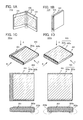
- FIG. 1A is a perspective view of a display device 110 that is being opened
- FIG. 1B is a perspective view of the display device 110 that is folded.
- the display device 110 includes a housing 103 and two display units 101 .
- the two display units 101 may have the same structure or different structures.
- the housing 103 is foldable.
- the housing 103 includes a joint portion 106 (e.g., a hinge) positioned between the two display units 101 (specifically, the joint portion 106 overlaps with part of the two display units 101 between the two display units 101 ).
- the housing 103 supports the two display units 101 .
- FIG. 1A shows an example in which the housing 103 has a depressed portion and the display units 101 are placed in the depressed portion.
- the display units 101 may be bonded to the housing 103 or may be detachably mounted thereon.
- the display device 110 is foldable. Accordingly, a user can fold the display device 110 into a small shape and carry it easily. Further, the user can view large-screen display by opening the display device 110 and using the two display units as one screen. Moreover, even when the display device 110 is opened and closed repeatedly, the display unit 101 itself is not deformed. In other words, for example, a decrease in the lifetime of the display unit 101 due to deformation is reduced and the display device 110 has high reliability.
- FIGS. 1C and 1D each illustrate an example of a structure of the display unit 101 .
- FIG. 1C shows a perspective view of a display unit 101 a and plan views seen in the directions of arrow A and arrow B in the perspective view.
- FIG. 1D shows a perspective view of a display unit 101 b and plan views seen in the directions of arrow A and arrow B in the perspective view.
- the display units 101 a and 101 b each include a support 201 and a display panel 203 .
- the display panel 203 has a display region 203 a and a non-display region 203 b.
- the display region 203 a overlaps with a first surface of the support 201 that can be viewed in the direction of arrow A in the perspective view
- the non-display region 203 b overlaps with a second surface of the support 201 that can be viewed in the direction of arrow C in the perspective view
- the non-display region 203 b overlaps with a third surface of the support 201 that is opposite to the second surface.
- the non-display region 203 b in the display panel 203 is indicated by dotted circles.
- the non-display region is provided to surround the display region.
- one of two surfaces in series of the support 201 (first surface) is overlapped with the display region 203 a
- the other (second surface) is overlapped with the non-display region 203 b .
- the proportion of the area of the first surface occupied by the display region 203 a is increased and the display unit can have a narrow bezel, as compared with the case where the display panel 203 overlaps with only one surface of the support 201 .
- the display panel 203 overlaps with three or more surfaces of the support 201 and the non-display region 203 b overlaps with the two separate surfaces among three surfaces in series of the support 201 (second and third surfaces) and the display region 203 a overlaps with the surface between the two separate surfaces (first surface), as in the display unit 101 b , the proportion of the area of the first surface occupied by the display region 203 a is further increased and the display unit can have a narrower bezel.
- the non-display region 203 b may overlap with the surface opposite to the first surface.
- the non-display region 203 b can overlap with the surface of the support 201 opposite to the first surface and the surface meeting the first surface (the second surface or the third surface); accordingly, a bezel of a display panel included in a display unit of one embodiment of the present invention does not need to be narrow.
- a bezel of a display panel included in a display unit of one embodiment of the present invention does not need to be narrow.
- the wider the area of the non-display region 203 b surrounding the display region 203 a is, the longer the distance between the edge of the display panel and the organic EL element is. This is preferable because an impurity such as moisture or oxygen is less likely to enter (or reach) the organic EL element from the outside of the display panel, leading to higher reliability of the display panel.
- a region 301 is a region of the display panel that overlaps with the first surface of the support 201
- a region 303 is a region of the display panel that overlaps with the surface of the support 201 opposite to the first surface or the surface meeting the first surface (the second surface or the third surface).
- the area of the display region 203 a is the same.
- the display region 203 a is entirely included in a region overlapping with the first surface.
- the region 303 is wider than in FIG. 7A . This is preferable because an external impurity such as moisture or oxygen is less likely to reach the organic EL element through the edge of the display panel.
- the area of a region where the display panel 203 overlaps with the surface of the support 201 opposite to the first surface is preferably 10% or more, further preferably 30% or more, still further preferably 50% or more of the area of the surface opposite to the first surface.
- the display region 203 a preferably overlaps with the second surface as well as the first surface.
- the display units 101 a and 101 b are used for the display units 101 in FIG. 1A , in the vicinity of a region where the two display units 101 are in contact with each other, almost no non-display region exists between the display region 203 a in one display unit and the display region 203 a in the other display unit. Therefore, display of the display device is less likely to appear divided when the two display units 101 are used as one screen.
- the display region 203 a preferably overlaps with the third surface, in which case the proportion of the area of the first surface occupied by the display region 203 a is increased.
- FIG. 2A is a plan view of a display device 120 that is opened.
- FIG. 2B is a plan view of the display device 120 that is folded.
- FIG. 2C is a perspective view of the display device 120 that is opened.
- FIG. 2D is a perspective view of the display device 120 that is folded.
- the display device 120 includes a housing 103 a and two display units (each display unit includes the support 201 and the display panel 203 ). The distance between the two display units is adjustable. In a display device of one embodiment of the present invention, at least one of two display units can be moved in the lateral direction of FIG. 2A .
- the display device 120 is shown as an example in which both of the two display units can be moved in the lateral direction of FIG. 2A .
- each of the two display units is a display unit 101 c shown in FIG. 3A ; however, one embodiment of the present invention is not limited thereto.
- any of the display units 101 a and 101 b shown in FIGS. 1C and 1D and a display unit 101 d shown in FIG. 3B can be used.
- one of the two display units may be the display unit 101 a and the other may be the display unit 101 c .
- the structure of the display unit 101 c is the same as that of the display unit 101 a except for having a projection 205
- the structure of the display unit 101 d is the same as that of the display unit 101 b except for having the projection 205 .
- FIG. 6A shows a perspective view and a plan view of the housing 103 a .
- the housing 103 a is foldable.
- the housing 103 a includes the joint portion 106 positioned between the two display units.
- the housing 103 a has a depressed portion and supports two display units placed in the depressed portion.
- FIGS. 2A to 2D show an example in which display units are detachably placed in the depressed portion of the housing 103 a.
- the two display units can be moved in the lateral direction of the drawing and can be fixed to the housing 103 a with the projection 205 (e.g., a nail, a hook, a lug, a tab, or a claw) of the support 201 and a projection 207 (e.g., a nail, a hook, a lug, a tab, or a claw) of the housing 103 a .
- the projection 205 and the projection 207 is provided in contact with the bottom surface or a side surface of the depressed portion of the housing 103 a.
- FIGS. 2A to 2D show a state where the two display units are apart from each other. It is possible to bring the two display units in contact with or close to each other by moving at least one of the display units. Such a state will be described in detail using a display device 140 shown later in drawings.
- the two display units are preferably in contact with each other.
- the two display units are preferably placed in the housing 103 a in an opened state to be in contact with each other such that the second surfaces of the supports 201 face each other. In that case, display is less likely to appear divided when the two display units are used as one screen.
- the positions of the two display units are not particularly limited.
- the two display units are preferably apart from each other.
- the edges of the display units do not exist on the same plane as the edge of the folded housing 103 a at the side surface including the joint portion 106 of the display device, which is shown in FIG. 2D ; thus, the supports 201 and the display panels 203 can be prevented from being damaged and broken.
- the display device is folded such that the display units are placed on the inner side of the display device; however, one embodiment of the present invention is not limited thereto.
- a display device 130 shown in FIG. 3C is folded such that the display units are placed on the outer side of the display device. Accordingly, even in the folded state, the display units on two opposite surfaces of the display device 130 can independently perform display.
- a display device of one embodiment of the present invention can be folded such that the display units are on either the outer side or the inner side of the display device. With such a structure, it is possible not only to open the display device and view the display on the display units but also to fold the display device such that the display units are on the outer side of the display device and view the display on the display units. Further, folding the display device such that the display units are on the inner side of the display device enables the display panels to be prevented from being damaged and broken when the display device is not in use.
- FIG. 4A and FIG. 5A are plan views of the display device 140 that is opened.
- FIG. 4B and FIG. 5B are perspective views of the display device 140 that is opened.
- FIG. 5C is a perspective view of the display device 140 that is folded.
- FIGS. 4A and 4B show the case where two display units are not in contact with each other, and FIGS. 5A to 5C show the case where two display units are in contact with each other.
- the display device 140 includes a housing 103 b and two display units (each display unit includes the support 201 and the display panel 203 ).
- each of the two display units is the display unit 101 c shown in FIG. 3A .
- FIG. 6B shows a perspective view and a plan view of the housing 103 b .
- the housing 103 b is foldable.
- the housing 103 b includes the joint portion 106 positioned between the two display units.
- the housing 103 b has a groove portion (depressed portion) and supports two display units placed in the groove portion.
- FIGS. 4A and 4B and FIGS. 5A to 5C show examples in which the display units are detachably placed in the groove portion of the housing 103 b .
- the housing 103 b covers part of the first surface of each support 201 (preferably, a portion overlapped with the non-display region of the display panel 203 ). Thus, the display device is less likely to be broken down into the display units and the housing.
- the two display units can be moved in the lateral direction of the drawing and can be fixed to the housing 103 b with the projection 205 (e.g., a nail, a hook, a lug, a tab, or a claw) of the support 201 and the projection 207 (e.g., a nail, a hook, a lug, a tab, or a claw) of the housing 103 b.
- the projection 205 e.g., a nail, a hook, a lug, a tab, or a claw
- the projection 207 e.g., a nail, a hook, a lug, a tab, or a claw
- the two display units are preferably in contact with each other, as shown in FIGS. 5A and 5B .
- the two display units are preferably placed in the housing 103 b in an opened state to be in contact with each other such that the second surfaces of the supports 201 face each other. In that case, display is less likely to appear divided when the two display units are used as one screen.
- the two display units are preferably apart from each other (refer to the perspective view of the display device 120 in FIG. 2D ).
- the edges of the display units exist on the same plane as the edge of the folded housing 103 b at the side surface including the joint portion 106 of the display device; thus, the supports 201 and the display panels 203 are damaged and broken in some cases.
- the housing and the support can be formed using plastic, a metal, an alloy, rubber, or the like.
- Plastic, rubber, or the like is preferably used because it can form a housing or a support that is lightweight and less likely to be broken.
- any of a variety of adhesives can be used, and for example, a resin that is curable at room temperature (e.g., a two-component-mixture-type resin), a light curable resin, a thermosetting resin, or the like can be used. Alternatively, a sheet-like adhesive may be used.
- a resin that is curable at room temperature e.g., a two-component-mixture-type resin
- a light curable resin e.g., a thermosetting resin, or the like
- a sheet-like adhesive may be used.
- the display panel preferably has flexibility. Note that the display panel does not necessarily have flexibility. For example, a display panel that is shaped in advance to fit the shape of the display device may be used.
- the display element included in the display panel for which a liquid crystal element, a light-emitting element (such as a light-emitting diode, an organic EL element, or an inorganic EL element), a plasma tube, or the like can be used.
- an organic EL element it is preferable to use an organic EL element because it makes it easy to provide a lightweight flexible display panel.
- the display panel may be an active matrix type or a passive matrix type.
- the structure of a transistor included in the display panel is not limited, and either a top-gate transistor or a bottom-gate transistor may be used. In addition, either an n-channel transistor or a p-channel transistor may be used. Furthermore, there is no particular limitation on a material used for the transistor. For example, a transistor in which silicon or an oxide semiconductor such as an In—Ga—Zn-based metal oxide is used in a channel formation region can be employed.
- the display panel may include a sensor such as a touch sensor.
- a substrate included in the display panel is preferably formed using a material with high toughness.
- a display panel with high impact resistance that is less likely to be broken can be provided.
- the display panel can be lightweight and less likely to be broken as compared with the case where a glass substrate is used.
- a flexible display panel can be manufactured using a variety of manufacturing methods. It is possible to form elements (e.g., a display element, a transistor, and a color filter) directly over a flexible substrate in the case where the flexible substrate can withstand the temperatures in the manufacturing process.
- elements e.g., a display element, a transistor, and a color filter
- a flexible display panel can be manufactured by a technique in which some components of a display panel are formed over a formation substrate having high heat resistance, and then the components are transferred from the formation substrate to a flexible substrate. Since a transistor and the like can be formed over a formation substrate having high heat resistance, a highly reliable transistor and an insulating layer with sufficiently low water permeability can be formed. Further, these components are transferred to a flexible substrate. In this manner, a flexible display panel with high reliability can be manufactured.
- a material which is flexible but has high water permeability and low heat resistance e.g., resin
- FIGS. 8A and 8B a flexible display panel that can be used for the display device of one embodiment of the present invention is described with reference to FIGS. 8A and 8B , FIGS. 9A and 9B , FIGS. 10A and 10B , FIGS. 11A and 11B , FIGS. 12A to 12C , and FIGS. 13A to 13C .
- the minimum curvature radius of a bent portion of the display panel can be greater than or equal to 1 mm and less than or equal to 150 mm, greater than or equal to 1 mm and less than or equal to 100 mm, greater than or equal to 1 mm and less than or equal to 50 mm, greater than or equal to 1 mm and less than or equal to 10 mm, or greater than or equal to 2 mm and less than or equal to 5 mm.
- the display panel in this embodiment is free from breakage of an element even when bent with a small curvature radius (e.g., greater than or equal to 2 mm and less than or equal to 5 mm) and has high reliability.
- Bending the display panel with a small curvature radius can make the display device of one embodiment of the present invention thin. Bending a light extraction portion 224 with a large curvature radius (e.g., greater than or equal to 5 mm and less than or equal to 100 mm) can provide a large display portion on a side surface of the display device. There is no limitation on the direction in which the display panel in this embodiment is bent. Further, the number of bent portions may be one or more than one.
- FIG. 8A is a plan view of a display panel
- FIG. 8B is an example of a cross-sectional view taken along dashed-dotted line A 1 -A 2 in FIG. 8A .
- the display panel in FIG. 8B includes a substrate 221 , a bonding layer 223 , an insulating layer 225 , a plurality of transistors, a conductive layer 157 , an insulating layer 227 , an insulating layer 229 , a plurality of light-emitting elements, an insulating layer 211 , a sealing layer 213 , an insulating layer 261 , a coloring layer 259 , a light-blocking layer 257 , an insulating layer 255 , a bonding layer 258 , and a substrate 222 .
- the conductive layer 157 is electrically connected to an FPC 228 via a connector 215 .
- a light-emitting element 230 includes a lower electrode 231 , an EL layer 233 , and an upper electrode 235 .
- the lower electrode 231 is electrically connected to a source electrode or a drain electrode of a transistor 240 .
- An end portion of the lower electrode 231 is covered with the insulating layer 211 .
- the light-emitting element 230 has a top emission structure.
- the upper electrode 235 has a light-transmitting property and transmits light emitted from the EL layer 233 .
- the coloring layer 259 is provided to overlap with the light-emitting element 230
- the light-blocking layer 257 is provided to overlap with the insulating layer 211 .
- the coloring layer 259 and the light-blocking layer 257 are covered with the insulating layer 261 .
- the space between the light-emitting element 230 and the insulating layer 261 is filled with the sealing layer 213 .
- the display panel includes a plurality of transistors in the light extraction portion 224 and a driver circuit portion 226 .
- the transistor 240 is provided over the insulating layer 225 .
- the insulating layer 225 and the substrate 221 are attached to each other with the bonding layer 223 .
- the insulating layer 255 and the substrate 222 are attached to each other with the bonding layer 258 . It is preferable to use films with low water permeability for the insulating layer 225 and the insulating layer 255 , in which case an impurity such as water can be prevented from entering the light-emitting element 230 or the transistor 240 , leading to improved reliability of the display panel.
- a film containing nitrogen and silicon e.g., a silicon nitride film or a silicon nitride oxide film
- a film containing nitrogen and aluminum e.g., an aluminum nitride film
- a silicon oxide film, a silicon oxynitride film, an aluminum oxide film, or the like can be used.
- the water vapor transmittance of the insulating film with low water permeability is lower than or equal to 1 ⁇ 10 ⁇ 5 [g/m 2 ⁇ day], preferably lower than or equal to 1 ⁇ 10 ⁇ 6 [g/m 2 ⁇ day], further preferably lower than or equal to 1 ⁇ 10 ⁇ 7 [g/m 2 ⁇ day], still further preferably lower than or equal to 1 ⁇ 10 ⁇ 8 [g/m 2 ⁇ day].
- the display panel in Specific Example 1 can be manufactured in the following manner: the insulating layer 225 , the transistor 240 , and the light-emitting element 230 are formed over a formation substrate with high heat resistance; the formation substrate is separated; and the insulating layer 225 , the transistor 240 , and the light-emitting element 230 are transferred to the substrate 221 and attached thereto with the bonding layer 223 .
- the display panel in Specific Example 1 can be manufactured in the following manner: the insulating layer 255 , the coloring layer 259 , and the light-blocking layer 257 are formed over a formation substrate with high heat resistance; the formation substrate is separated; and the insulating layer 255 , the coloring layer 259 , and the light-blocking layer 257 are transferred to the substrate 222 and attached thereto with the bonding layer 258 .
- a material with low heat resistance e.g., resin
- a material with high water permeability e.g., resin
- a transistor and the like can be formed over a formation substrate having high heat resistance; thus, the substrate can be exposed to high temperature and a highly reliable transistor and an insulating film with sufficiently low water permeability can be formed. Then, the transistor and the insulating film are transferred to a substrate with low heat resistance, whereby a highly reliable display panel can be manufactured.
- a thin or/and lightweight display panel with high reliability can be provided. Details of the manufacturing method will be described later.
- the substrate 221 and the substrate 222 are each preferably formed using a material with high toughness.
- a display panel with high impact resistance that is less likely to be broken can be provided.
- the substrate 222 is an organic resin substrate and the substrate 221 is a substrate formed using a thin metal material or a thin alloy material
- the display panel can be lightweight and less likely to be broken as compared with the case where a glass substrate is used.
- a metal material and an alloy material, which have high thermal conductivity, are preferred because they can easily conduct heat to the whole substrate and accordingly can prevent a local temperature rise in the display panel.
- the thickness of a substrate using a metal material or an alloy material is preferably greater than or equal to 10 ⁇ m and less than or equal to 200 ⁇ m, further preferably greater than or equal to 20 ⁇ m and less than or equal to 50 ⁇ m.
- the substrate 221 may have a stacked structure of a metal substrate and a layer with high thermal emissivity (the layer can be formed using a metal oxide or a ceramic material, for example).
- FIG. 9A shows another example of the light extraction portion 224 in the display panel of one embodiment of the present invention.
- the display panel shown in FIG. 9A is capable of touch operation.
- description of components similar to those in Specific Example 1 is omitted.
- the display panel in FIG. 9A includes the substrate 221 , the bonding layer 223 , the insulating layer 225 , a plurality of transistors, the insulating layer 227 , the insulating layer 229 , a plurality of light-emitting elements, the insulating layer 211 , an insulating layer 217 , the sealing layer 213 , the insulating layer 261 , the coloring layer 259 , the light-blocking layer 257 , a plurality of light-receiving elements, a conductive layer 281 , a conductive layer 283 , an insulating layer 291 , an insulating layer 293 , an insulating layer 295 , the insulating layer 255 , the bonding layer 258 , and the substrate 222 .
- Specific Example 2 includes the insulating layer 217 over the insulating layer 211 .
- the space between the substrate 222 and the substrate 221 can be adjusted with the insulating layer 217 .
- FIG. 9A shows an example in which a light-receiving element is provided between the insulating layer 255 and the sealing layer 213 . Since the light-receiving element can be placed to overlap with a non-light-emitting region (e.g., a region where the light-emitting element is not provided, such as a region where a transistor or a wiring is provided) of the display panel, the display panel can be provided with a touch sensor without a decrease in the aperture ratio of a pixel (light-emitting element).
- a non-light-emitting region e.g., a region where the light-emitting element is not provided, such as a region where a transistor or a wiring is provided
- a PN photodiode or a PIN photodiode can be used as the light-receiving element included in the display panel of one embodiment of the present invention.
- a PIN photodiode including a p-type semiconductor layer 271 , an i-type semiconductor layer 273 , and an n-type semiconductor layer 275 is used as the light-receiving element.
- the i-type semiconductor layer 273 is a semiconductor in which the concentration of each of an impurity imparting p-type conductivity and an impurity imparting n-type conductivity is 1 ⁇ 10 20 cm ⁇ 3 or less and which has photoconductivity 100 times or more as high as dark conductivity.
- the i-type semiconductor layer 273 also includes, in its category, a semiconductor that contains an impurity element belonging to Group 13 or Group 15 of the periodic table.
- the i-type semiconductor layer 273 includes, in its category, a semiconductor to which an impurity element imparting p-type conductivity is added intentionally or unintentionally at the time of deposition or after the deposition.
- the light-blocking layer 257 is closer to the substrate 221 than is the light-receiving element and overlaps with the light-receiving element.
- the light-blocking layer 257 between the light-receiving element and the sealing layer 213 can prevent the light-receiving element from being irradiated with light emitted from the light-emitting element 230 .
- the conductive layer 281 and the conductive layer 283 are electrically connected to the light-receiving element.
- the conductive layer 281 preferably transmits light incident on the light-receiving element.
- the conductive layer 283 preferably blocks light incident on the light-receiving element.
- optical touch sensor between the substrate 222 and the sealing layer 213 because the optical touch sensor is less likely to be affected by light emitted from the light-emitting element 230 and can have improved S/N ratio.
- FIG. 9B shows another example of the light extraction portion 224 in the display panel of one embodiment of the present invention.
- the display panel shown in FIG. 9B is capable of touch operation.
- the display panel in FIG. 9B includes the substrate 221 , the bonding layer 223 , the insulating layer 225 , a plurality of transistors, the insulating layer 227 , an insulating layer 229 a , an insulating layer 229 b , a plurality of light-emitting elements, the insulating layer 211 , the insulating layer 217 , the sealing layer 213 , the coloring layer 259 , the light-blocking layer 257 , a plurality of light-receiving elements, a conductive layer 280 , the conductive layer 281 , the insulating layer 255 , the bonding layer 258 , and the substrate 222 .
- FIG. 9B shows an example in which a light-receiving element is provided between the insulating layer 225 and the sealing layer 213 . Since the light-receiving element is provided between the insulating layer 225 and the sealing layer 213 , a conductive layer to which the light-receiving element is electrically connected and a photoelectric conversion layer included in the light-receiving element can be formed using the same materials and the same steps as a conductive layer and a semiconductor layer included in the transistor 240 . Thus, the display panel capable of touch operation can be manufactured without a significant increase in the number of manufacturing steps.
- FIG. 10A shows another example of a display panel of one embodiment of the present invention.
- the display panel shown in FIG. 10A is capable of touch operation.
- the display panel in FIG. 10A includes the substrate 221 , the bonding layer 223 , the insulating layer 225 , a plurality of transistors, a conductive layer 156 , the conductive layer 157 , the insulating layer 227 , the insulating layer 229 , a plurality of light-emitting elements, the insulating layer 211 , the insulating layer 217 , the sealing layer 213 , the coloring layer 259 , the light-blocking layer 257 , the insulating layer 255 , a conductive layer 272 , a conductive layer 274 , an insulating layer 276 , an insulating layer 278 , a conductive layer 294 , a conductive layer 296 , the bonding layer 258 , and the substrate 222 .
- FIG. 10A shows an example in which a capacitive touch sensor is provided between the insulating layer 255 and the sealing layer 213 .
- the capacitive touch sensor includes the conductive layer 272 and the conductive layer 274 .
- the conductive layer 156 and the conductive layer 157 are electrically connected to the FPC 228 via the connector 215 .
- the conductive layer 294 and the conductive layer 296 are electrically connected to the conductive layer 274 via conductive particles 292 .
- the capacitive touch sensor can be driven via the FPC 228 .
- FIG. 10B shows another example of a display panel of one embodiment of the present invention.
- the display panel shown in FIG. 10B is capable of touch operation.
- the display panel in FIG. 10B includes the substrate 221 , the bonding layer 223 , the insulating layer 225 , a plurality of transistors, the conductive layer 156 , the conductive layer 157 , the insulating layer 227 , the insulating layer 229 , a plurality of light-emitting elements, the insulating layer 211 , the insulating layer 217 , the sealing layer 213 , the coloring layer 259 , the light-blocking layer 257 , the insulating layer 255 , a conductive layer 270 , the conductive layer 272 , the conductive layer 274 , the insulating layer 276 , the insulating layer 278 , the bonding layer 258 , and the substrate 222 .
- FIG. 10B shows an example in which a capacitive touch sensor is provided between the insulating layer 255 and the sealing layer 213 .
- the capacitive touch sensor includes the conductive layer 272 and the conductive layer 274 .
- the conductive layer 156 and the conductive layer 157 are electrically connected to an FPC 228 a via a connector 215 a .
- the conductive layer 270 is electrically connected to an FPC 228 b via a connector 215 b .
- the light-emitting element 230 and the transistor 240 can be driven via the FPC 228 a
- the capacitive touch sensor can be driven via the FPC 228 b.
- FIG. 11A shows another example of the light extraction portion 224 in the display panel of one embodiment of the present invention.
- the display panel in FIG. 11A includes the substrate 222 , the bonding layer 258 , the insulating layer 225 , a plurality of transistors, the insulating layer 227 , a conductive layer 237 , the insulating layer 229 a , the insulating layer 229 b , a plurality of light-emitting elements, the insulating layer 211 , the sealing layer 213 , the coloring layer 259 , and a substrate 239 .
- the light-emitting element 230 includes the lower electrode 231 , the EL layer 233 , and the upper electrode 235 .
- the lower electrode 231 is electrically connected to the source electrode or the drain electrode of the transistor 240 via the conductive layer 237 .
- An end portion of the lower electrode 231 is covered with the insulating layer 211 .
- the light-emitting element 230 has a bottom emission structure.
- the lower electrode 231 has a light-transmitting property and transmits light emitted from the EL layer 233 .
- the coloring layer 259 is provided to overlap with the light-emitting element 230 , and light emitted from the light-emitting element 230 is extracted from the substrate 222 side through the coloring layer 259 .
- the space between the light-emitting element 230 and the substrate 239 is filled with the sealing layer 213 .
- the substrate 239 can be formed using a material similar to that of the substrate 221 .
- FIG. 11B shows another example of a display panel of one embodiment of the present invention.
- the display panel in FIG. 11B includes the substrate 222 , the bonding layer 258 , the insulating layer 225 , a conductive layer 310 a , a conductive layer 310 b , a plurality of light-emitting elements, the insulating layer 211 , a conductive layer 212 , the sealing layer 213 , and the substrate 239 .
- the conductive layer 310 a and the conductive layer 310 b which are external connection electrodes of the display panel, can each be electrically connected to an FPC or the like.
- the light-emitting element 230 includes the lower electrode 231 , the EL layer 233 , and the upper electrode 235 . An end portion of the lower electrode 231 is covered with the insulating layer 211 .
- the light-emitting element 230 has a bottom emission structure.
- the lower electrode 231 has a light-transmitting property and transmits light emitted from the EL layer 233 .
- the conductive layer 212 is electrically connected to the lower electrode 231 .
- the substrate 222 may have, as a light extraction structure, a hemispherical lens, a micro lens array, a film provided with an uneven surface structure, a light diffusing film, or the like.
- the substrate 222 with a light extraction structure can be formed by attaching the above lens or film to a resin substrate with an adhesive or the like having substantially the same refractive index as the substrate or the lens or film.
- the conductive layer 212 is preferably, though not necessarily, provided because voltage drop due to the resistance of the lower electrode 231 can be prevented.
- a conductive layer electrically connected to the upper electrode 235 may be provided over the insulating layer 211 , the EL layer 233 , the upper electrode 235 , or the like.
- the conductive layer 212 can be a single layer or a stacked layer formed using a material selected from copper, titanium, tantalum, tungsten, molybdenum, chromium, neodymium, scandium, nickel, or aluminum, an alloy material containing any of these materials as its main component, or the like.
- the thickness of the conductive layer 212 can be, for example, greater than or equal to 0.1 ⁇ m and less than or equal to 3 ⁇ m, preferably greater than or equal to 0.1 ⁇ m and less than or equal to 0.5 ⁇ m.
- a paste e.g., silver paste
- metal particles forming the conductive layer aggregate; therefore, the surface of the conductive layer is rough and has many gaps.
- the conductive layer is formed over the insulating layer 211 , for example, it is difficult for the EL layer 233 to completely cover the conductive layer; accordingly, the upper electrode and the conductive layer are electrically connected to each other easily, which is preferable.
- Examples of materials used for the substrate 221 , the substrate 222 , and the substrate 239 include glass, a metal, and an organic resin. A material that transmits visible light is used for the substrate on the display surface side of the display panel.
- An organic resin which has a specific gravity smaller than that of glass, is preferably used for the substrate, in which case the display panel can be lightweight as compared with the case where glass is used.
- Examples of a material having flexibility and a light-transmitting property with respect to visible light include glass that is thin enough to have flexibility, polyester resins such as polyethylene terephthalate (PET) and polyethylene naphthalate (PEN), a polyacrylonitrile resin, a polyimide resin, a polymethyl methacrylate resin, a polycarbonate (PC) resin, a polyethersulfone (PES) resin, a polyamide resin, a cycloolefin resin, a polystyrene resin, a polyamide imide resin, and a polyvinyl chloride resin.
- PET polyethylene terephthalate
- PEN polyethylene naphthalate
- PES polyethersulfone
- a material whose thermal expansion coefficient is low is preferred, and for example, a polyamide imide resin, a polyimide resin, or PET can be suitably used.
- a substrate in which a glass fiber is impregnated with an organic resin or a substrate whose thermal expansion coefficient is reduced by mixing an organic resin with an inorganic filler can also be used.
- the substrate may have a stacked structure of a layer of any of the above-mentioned materials and a hard coat layer (e.g., a silicon nitride layer) which protects a surface of the display panel from damage or the like, a layer (e.g., an aramid resin layer) which can disperse pressure, or the like. Furthermore, to suppress a decrease in the lifetime of the light-emitting element due to moisture and the like, an insulating film with low water permeability may be included in the stacked structure.
- a hard coat layer e.g., a silicon nitride layer
- a layer e.g., an aramid resin layer
- an insulating film with low water permeability may be included in the stacked structure.
- a material that transmits visible light is used for one of the bonding layer 223 and the bonding layer 258 that is on the display surface side of the display panel.
- a resin that is curable at room temperature e.g., a two-component-mixture-type resin
- a light curable resin e.g., a thermosetting resin, or the like
- resins include an epoxy resin, an acrylic resin, a silicone resin, and a phenol resin.
- a material with low moisture permeability such as an epoxy resin, is preferred.
- the resin may include a drying agent.
- a substance that adsorbs moisture by chemical adsorption such as oxide of an alkaline earth metal (e.g., calcium oxide or barium oxide)
- an alkaline earth metal e.g., calcium oxide or barium oxide
- a substance that adsorbs moisture by physical adsorption such as zeolite or silica gel
- the drying agent is preferably included because it can prevent an impurity such as moisture from entering the light-emitting element, thereby improving the reliability of the display panel.
- a filler with a high refractive index e.g., titanium oxide
- a high refractive index e.g., titanium oxide
- the bonding layer may also include a scattering member for scattering light.
- the bonding layer can be a mixture of the above resin and particles having a refractive index different from that of the resin. The particles function as the scattering member for scattering light.
- the difference in refractive index between the resin and the particles with a refractive index different from that of the resin is preferably 0.1 or more, further preferably 0.3 or more.
- an epoxy resin, an acrylic resin, an imide resin, silicone, or the like can be used as the resin, and titanium oxide, barium oxide, zeolite, or the like can be used as the particles.
- Particles of titanium oxide or barium oxide are preferable because they scatter light excellently.
- zeolite When zeolite is used, it can adsorb water contained in the resin and the like, thereby improving the reliability of the light-emitting element.
- the structure of the transistors in the display panel is not particularly limited.
- a forward staggered transistor or an inverted staggered transistor may be used.
- a top-gate transistor or a bottom-gate transistor may be used.
- a semiconductor material used for the transistors is not particularly limited, and for example, silicon or germanium can be used.
- an oxide semiconductor containing at least one of indium, gallium, and zinc, such as an In—Ga—Zn-based metal oxide, may be used.
- crystallinity of a semiconductor material used for the transistors there is no particular limitation on the crystallinity of a semiconductor material used for the transistors, and an amorphous semiconductor or a semiconductor having crystallinity (a microcrystalline semiconductor, a polycrystalline semiconductor, a single-crystal semiconductor, or a semiconductor partly including crystal regions) may be used. It is preferable that a semiconductor having crystallinity be used, in which case deterioration of the transistor characteristics can be suppressed.
- the light-emitting element included in the display panel includes a pair of electrodes (the lower electrode 231 and the upper electrode 235 ); and the EL layer 233 between the pair of electrodes.
- One of the pair of electrodes functions as an anode and the other functions as a cathode.
- the light-emitting element may have any of a top emission structure, a bottom emission structure, and a dual emission structure.
- a conductive film that transmits visible light is used as the electrode through which light is extracted.
- a conductive film that reflects visible light is preferably used as the electrode through which light is not extracted.
- the conductive film that transmits visible light can be formed using, for example, indium oxide, indium tin oxide (ITO), indium zinc oxide, zinc oxide, or zinc oxide to which gallium is added.
- a film of a metal material such as gold, silver, platinum, magnesium, nickel, tungsten, chromium, molybdenum, iron, cobalt, copper, palladium, or titanium; an alloy containing any of these metal materials; or a nitride of any of these metal materials (e.g., titanium nitride) can be formed thin so as to have a light-transmitting property.
- a stack of any of the above materials can be used as the conductive film.
- a stacked film of ITO and an alloy of silver and magnesium is preferably used, in which case conductivity can be increased.
- graphene or the like may be used.
- a metal material such as aluminum, gold, platinum, silver, nickel, tungsten, chromium, molybdenum, iron, cobalt, copper, or palladium or an alloy containing any of these metal materials can be used.
- lanthanum, neodymium, germanium, or the like may be added to the metal material or the alloy.
- an alloy containing aluminum such as an alloy of aluminum and titanium, an alloy of aluminum and nickel, or an alloy of aluminum and neodymium; or an alloy containing silver such as an alloy of silver and copper, an alloy of silver, copper, and palladium, or an alloy of silver and magnesium can be used for the conductive film.
- An alloy of silver and copper is preferable because of its high heat resistance. Further, when a metal film or a metal oxide film is stacked on and in contact with an aluminum alloy film, oxidation of the aluminum alloy film can be prevented. Examples of a material for the metal film or the metal oxide film are titanium and titanium oxide. Alternatively, the above conductive film that transmits visible light and a film containing a metal material may be stacked. For example, a stacked film of silver and ITO or a stacked film of an alloy of silver and magnesium and ITO can be used.
- Each of the electrodes can be formed by an evaporation method or a sputtering method.
- a discharging method such as an inkjet method, a printing method such as a screen printing method, or a plating method may be used.
- the EL layer 233 includes at least a light-emitting layer.
- the EL layer 233 may further include one or more layers containing any of a substance with a high hole-injection property, a substance with a high hole-transport property, a hole-blocking material, a substance with a high electron-transport property, a substance with a high electron-injection property, a substance with a bipolar property (a substance with a high electron- and hole-transport property), and the like.
- a low molecular compound or a high molecular compound can be used, and an inorganic compound may also be used.
- Each of the layers included in the EL layer 233 can be formed by any of the following methods: an evaporation method (including a vacuum evaporation method), a transfer method, a printing method, an inkjet method, a coating method, and the like.
- the insulating layer 225 and the insulating layer 255 can each be formed using an inorganic insulating material. It is particularly preferable to use an insulating film with low water permeability, in which case a highly reliable display panel can be provided.
- the insulating layer 227 has an effect of preventing diffusion of impurities into a semiconductor included in the transistor.
- an inorganic insulating film such as a silicon oxide film, a silicon oxynitride film, a silicon nitride film, a silicon nitride oxide film, or an aluminum oxide film can be used.
- an insulating film with a planarization function is preferably selected in order to reduce surface unevenness due to the transistor or the like.
- an organic material such as a polyimide resin, an acrylic resin, or a benzocyclobutene-based resin can be used.
- a low-dielectric constant material a low-k material
- the planarization insulating film may have a stacked structure of any of insulating films formed of these materials and inorganic insulating films.
- the insulating layer 211 is provided to cover an end portion of the lower electrode 231 .
- a side wall of the insulating layer 211 preferably has a tilted surface with continuous curvature.
- a resin or an inorganic insulating material can be used as a material for the insulating layer 211 .
- the resin for example, a polyimide resin, a polyamide resin, an acrylic resin, a siloxane resin, an epoxy resin, or a phenol resin can be used.
- a negative photosensitive resin or a positive photosensitive resin is preferably used for easy formation of the insulating layer 211 .
- a photolithography method e.g., a sputtering method, an evaporation method, a droplet discharging method (e.g., an inkjet method), a printing method (e.g., a screen printing method or an off-set printing method), or the like may be used.
- a photolithography method e.g., a sputtering method, an evaporation method, a droplet discharging method (e.g., an inkjet method), a printing method (e.g., a screen printing method or an off-set printing method), or the like may be used.
- the insulating layer 217 can be formed using an inorganic insulating material, an organic insulating material, or the like.
- the organic insulating material for example, a negative or positive photosensitive resin, a non-photosensitive resin, or the like can be used.
- a conductive layer may be formed.
- the conductive layer can be formed using a metal material such as titanium or aluminum.
- Each of the insulating layers 276 , 278 , 291 , 293 , and 295 can be formed using an inorganic insulating material or an organic insulating material. It is particularly preferable to use an insulating film with a planarization function for each of the insulating layers 278 and 295 in order to reduce surface unevenness due to a sensor element.
- a resin that is curable at room temperature e.g., a two-component-mixture-type resin
- a light curable resin e.g., a thermosetting resin, or the like
- a polyvinyl chloride (PVC) resin an acrylic resin, a polyimide resin, an epoxy resin, a silicone resin, a polyvinyl butyral (PVB) resin, an ethylene vinyl acetate (EVA) resin, or the like
- a drying agent may be contained in the sealing layer 213 .
- the sealing layer 213 preferably includes a filler with a high refractive index or a scattering member.
- Materials for the drying agent, the filler with a high refractive index, and the scattering member are similar to those that can be used for the bonding layer 258 .
- Each of the conductive layers 156 , 157 , 294 , and 296 can be formed using the same material and the same step as a conductive layer included in the transistor or the light-emitting element.
- the conductive layer 280 can be formed using the same material and the same step as a conductive layer included in the transistor.
- each of the conductive layers can be formed to have a single-layer structure or a stacked-layer structure using any of metal materials such as molybdenum, titanium, chromium, tantalum, tungsten, aluminum, copper, neodymium, and scandium, and an alloy material containing any of these elements.
- Each of the conductive layers may be formed using a conductive metal oxide.
- the conductive metal oxide indium oxide (e.g., In 2 O 3 ), tin oxide (e.g., SnO 2 ), zinc oxide (ZnO), ITO, indium zinc oxide (e.g., In 2 O 3 —ZnO), or any of these metal oxide materials in which silicon oxide is contained can be used.
- Each of the conductive layers 237 , 212 , 310 a , and 310 b can also be formed using any of the above metal materials, alloy materials, and conductive metal oxides.
- Each of the conductive layers 272 , 274 , 281 , and 283 is a conductive layer with a light-transmitting property.
- the conductive layer can be formed using, for example, indium oxide, ITO, indium zinc oxide, zinc oxide, zinc oxide to which gallium is added, or the like.
- the conductive layer 270 can be formed using the same material and the same step as the conductive layer 272 .
- the conductive particles 292 particles of an organic resin, silica, or the like coated with a metal material are used. It is preferable to use nickel or gold as the metal material because contact resistance can be reduced. It is also preferable to use particles each coated with layers of two or more kinds of metal materials, such as particles coated with nickel and further with gold.
- the connector 215 it is possible to use a paste-like or sheet-like material which is obtained by mixture of metal particles and a thermosetting resin and for which anisotropic electric conductivity is provided by thermocompression bonding.
- the metal particles particles in which two or more kinds of metals are layered, for example, nickel particles coated with gold are preferably used.
- the coloring layer 259 is a colored layer that transmits light in a specific wavelength range.
- a red (R) color filter for transmitting light in a red wavelength range a green (G) color filter for transmitting light in a green wavelength range, a blue (B) color filter for transmitting light in a blue wavelength range, or the like can be used.
- Each coloring layer is formed in a desired position with any of various materials by a printing method, an inkjet method, an etching method using a photolithography method, or the like.
- the light-blocking layer 257 is provided between the adjacent coloring layers 259 .
- the light-blocking layer 257 blocks light emitted from the adjacent light-emitting element, thereby preventing color mixture between adjacent pixels.
- the coloring layer 259 is provided such that its end portion overlaps with the light-blocking layer 257 , whereby light leakage can be reduced.
- the light-blocking layer 257 can be formed using a material that blocks light emitted from the light-emitting element, for example, a metal material, a resin material including a pigment or a dye, or the like.
- the light-blocking layer 257 is preferably provided in a region other than the light extraction portion 224 , such as the driver circuit portion 226 , as illustrated in FIG. 8B , in which case undesired leakage of guided light or the like can be prevented.
- the insulating layer 261 covering the coloring layer 259 and the light-blocking layer 257 is preferably provided because it can prevent an impurity such as a pigment included in the coloring layer 259 or the light-blocking layer 257 from diffusing into the light-emitting element or the like.
- a light-transmitting material is used, and an inorganic insulating material or an organic insulating material can be used.
- An insulating film with low water permeability may be used for the insulating layer 261 . Note that the insulating layer 261 is not necessarily provided.
- FIGS. 12A to 12C and FIGS. 13A to 13C an example of a method for manufacturing a display panel of one embodiment of the present invention will be described with reference to FIGS. 12A to 12C and FIGS. 13A to 13C .
- the manufacturing method is described using the display panel of Specific Example 1 ( FIG. 8B ) as an example.
- a separation layer 313 is formed over a formation substrate 311 , and the insulating layer 225 is formed over the separation layer 313 .
- the plurality of transistors, the conductive layer 157 , the insulating layer 227 , the insulating layer 229 , the plurality of light-emitting elements, and the insulating layer 211 are formed over the insulating layer 225 .
- An opening is formed in the insulating layers 211 , 229 , and 227 to expose the conductive layer 157 ( FIG. 12A ).
- a separation layer 307 is formed over a formation substrate 305 , and the insulating layer 255 is formed over the separation layer 307 .
- the light-blocking layer 257 , the coloring layer 259 , and the insulating layer 261 are formed over the insulating layer 255 ( FIG. 12B ).
- the formation substrate 311 and the formation substrate 305 can each be a glass substrate, a quartz substrate, a sapphire substrate, a ceramic substrate, a metal substrate, an organic resin substrate, or the like.
- a glass material such as aluminosilicate glass, aluminoborosilicate glass, or barium borosilicate glass can be used.
- a substrate having a strain point of 730° C. or higher is preferably used. Note that when containing a large amount of barium oxide, the glass substrate can be heat-resistant and more practical. Alternatively, crystallized glass or the like may be used.
- an insulating film such as a silicon oxide film, a silicon oxynitride film, a silicon nitride film, or a silicon nitride oxide film is preferably formed between the formation substrate and the separation layer, in which case contamination from the glass substrate can be prevented.
- the separation layer 313 and the separation layer 307 each have a single-layer structure or a stacked-layer structure containing an element selected from tungsten, molybdenum, titanium, tantalum, niobium, nickel, cobalt, zirconium, zinc, ruthenium, rhodium, palladium, osmium, iridium, and silicon; an alloy material containing any of the elements; or a compound material containing any of the elements.
- a crystal structure of a layer containing silicon may be amorphous, microcrystal, or polycrystal.
- the separation layer can be formed by a sputtering method, a plasma CVD method, a coating method, a printing method, or the like.
- a coating method includes a spin coating method, a droplet discharge method, and a dispensing method.
- a tungsten layer, a molybdenum layer, or a layer containing a mixture of tungsten and molybdenum is preferably formed.
- a layer containing an oxide or an oxynitride of tungsten, a layer containing an oxide or an oxynitride of molybdenum, or a layer containing an oxide or an oxynitride of a mixture of tungsten and molybdenum may be formed.
- the mixture of tungsten and molybdenum corresponds to an alloy of tungsten and molybdenum, for example.
- the layer containing an oxide of tungsten may be formed as follows: the layer containing tungsten is formed first and an insulating film formed of an oxide is formed thereover, so that the layer containing an oxide of tungsten is formed at the interface between the tungsten layer and the insulating film.
- the layer containing an oxide of tungsten may be formed by performing thermal oxidation treatment, oxygen plasma treatment, nitrous oxide (N 2 O) plasma treatment, treatment with a highly oxidizing solution such as ozone water, or the like on the surface of the layer containing tungsten.
- Plasma treatment or heat treatment may be performed in an atmosphere of oxygen, nitrogen, or nitrous oxide alone, or a mixed gas of any of these gasses and another gas.
- Surface condition of the separation layer is changed by the plasma treatment or heat treatment, whereby adhesion between the separation layer and the insulating layer formed later can be controlled.
- Each of the insulating layers can be formed by a sputtering method, a plasma CVD method, a coating method, a printing method, or the like.
- the insulating layer is formed at a temperature of higher than or equal to 250° C. and lower than or equal to 400° C. by a plasma CVD method, whereby the insulating layer can be a dense film with very low water permeability.
- a material for the sealing layer 213 is applied to a surface of the formation substrate 305 over which with the coloring layer 259 and the like are formed or a surface of the formation substrate 311 over which the light-emitting element 230 and the like are formed, and the formation substrate 311 and the formation substrate 305 are attached so that these two surfaces face each other with the sealing layer 213 positioned therebetween ( FIG. 12C ).
- the formation substrate 311 is separated, and the exposed insulating layer 225 and the substrate 221 are attached to each other with the bonding layer 223 . Further, the formation substrate 305 is separated, and the exposed insulating layer 255 and the substrate 222 are attached to each other with the bonding layer 258 . Although the substrate 222 does not overlap with the conductive layer 157 in FIG. 13A , the substrate 222 may overlap with the conductive layer 157 .
- any of a variety of methods can be used as appropriate for the separation process.
- the metal oxide film is embrittled by crystallization, whereby the layer to be separated can be separated from the formation substrate.
- an amorphous silicon film containing hydrogen is formed as the separation layer between the formation substrate having high heat resistance and the layer to be separated, the amorphous silicon film is removed by laser light irradiation or etching, whereby the layer to be separated can be separated from the formation substrate.
- the metal oxide film is embrittled by crystallization, and part of the separation layer is removed by etching using a solution or a fluoride gas such as NF 3 , BrF 3 , or ClF 3 , whereby the separation can be performed at the embrittled metal oxide film.
- a fluoride gas such as NF 3 , BrF 3 , or ClF 3
- a method may be used in which a film containing nitrogen, oxygen, hydrogen, or the like (for example, an amorphous silicon film containing hydrogen, an alloy film containing hydrogen, an alloy film containing oxygen, or the like) is used as the separation layer, and the separation layer is irradiated with laser light to release the nitrogen, oxygen, or hydrogen contained in the separation layer as a gas, thereby promoting separation between the layer to be separated and the formation substrate.
- a method in which the formation substrate provided with the layer to be separated is removed mechanically or by etching using a solution or a fluoride gas such as NF 3 , BrF 3 , or ClF 3 , or the like. In this case, the separation layer is not necessarily provided.
- the separation process can be conducted easily by combination of the above-described separation methods.
- separation can be performed with physical force (by a machine or the like) after performing laser light irradiation, etching on the separation layer with a gas, a solution, or the like, or mechanical removal with a sharp knife, scalpel or the like so that the separation layer and the layer to be separated can be easily separated from each other.
- Separation of the layer to be separated from the formation substrate may be carried out by filling the interface between the separation layer and the layer to be separated with a liquid. Further, the separation may be conducted while pouring a liquid such as water.
- the separation layer is formed using tungsten, it is preferable that the separation be performed while etching the separation layer using a mixed solution of ammonium water and a hydrogen peroxide solution.
- the separation layer is not necessary in the case where separation at the interface between the formation substrate and the layer to be separated is possible.
- glass is used as the formation substrate, an organic resin such as polyimide, polyester, polyolefin, polyamide, polycarbonate, or acrylic is formed in contact with the glass, and an insulating film, a transistor, and the like are formed over the organic resin.
- heating the organic resin enables the separation at the interface between the formation substrate and the organic resin.
- separation at the interface between a metal layer and the organic resin may be performed in the following manner: the metal layer is provided between the formation substrate and the organic resin and current is made to flow in the metal layer so that the metal layer is heated.
- an opening is formed in the insulating layer 255 and the sealing layer 213 to expose the conductive layer 157 ( FIG. 13B ).
- the opening is formed also in the substrate 222 and the bonding layer 258 so that the conductive layer 157 is exposed ( FIG. 13C ).
- the method for forming the opening is not particularly limited and may be, for example, a laser ablation method, an etching method, an ion beam sputtering method, or the like.
- a cut may be made in a film over the conductive layer 157 with a sharp knife or the like and part of the film may be separated by physical force.
- the display panel of one embodiment of the present invention can be manufactured.
- a display panel of one embodiment of the present invention includes two substrates; one is the substrate 222 and the other is the substrate 221 or the substrate 239 .
- the light-emitting device can be formed with two substrates even when including a touch sensor. Owing to the use of the minimum number of substrates, improvement in light extraction efficiency and improvement in clarity of display can be easily achieved.
- 101 display unit, 101 a : display unit, 101 b : display unit, 101 c : display unit, 101 d : display unit, 103 : housing, 103 a : housing, 103 b : housing, 106 : joint portion, 110 : display device, 120 : display device, 130 : display device, 140 : display device, 156 : conductive layer, 157 : conductive layer, 201 : support, 203 : display panel, 203 a : display region, 203 b : non-display region, 205 : projection, 207 : projection, 211 : insulating layer, 212 : conductive layer, 213 : sealing layer, 215 : connector, 215 a : connector, 215 b : connector, 217 : insulating layer, 221 : substrate, 222 : substrate, 223 : bonding layer, 224 : light extraction portion, 225 : insulating layer, 226 : driver circuit portion, 227
Abstract
Display of a display device is made less likely to appear divided when a plurality of display panels are used as one screen. Provided is a display device including two display units and a foldable housing that includes a joint portion between the two display units and supports the two display units. Each display unit includes a display panel including a display region and a non-display region and a support having a first surface overlapped with the display region and a second surface that meets the first surface and is overlapped with the non-display region. The two display units are placed in the housing in an opened state such that the first surfaces of the supports face the same direction and the second surfaces of the supports face each other.
Description
The present invention relates to a display device, an electronic device, or a manufacturing method thereof. The present invention particularly relates to a display device or an electronic device utilizing electroluminescence (hereinafter also referred to as EL) or a manufacturing method thereof.
Recent display devices are expected to be applied to a variety of uses and become diversified. For example, display devices for mobile devices and the like are required to be small, thin, and lightweight. In addition, display devices desirably have large screens (wide display regions), and a reduction in the area of a display device except a display region (what is called a narrower bezel) is required.
Light-emitting elements utilizing EL (also referred to as EL elements) have features such as ease of thinning and lightening, high-speed response to input signal, and driving with a direct-current low voltage source; therefore, application of the light-emitting elements to display devices has been proposed.
For example, Patent Document 1 discloses a foldable portable communication device that has reduced size and weight and that includes a plurality of displays and can be opened and closed so as to have a large screen.
- [Patent Document 1] Japanese Published Patent Application No. 2000-184026
However, since each display has a non-display region that surrounds a display region, in the structure of Patent Document 1, the non-display region exists at the joint between the two displays and in the vicinity thereof. The wider the non-display region is, the more divided an image displayed with the plurality of displays appears to a viewer.
An object of one embodiment of the present invention is to provide a novel display device or electronic device. Another object of one embodiment of the present invention is to provide a display device or an electronic device of which display is less likely to appear divided when a plurality of display panels are used as one screen. Another object of one embodiment of the present invention is to provide a small display device or electronic device. Another object of one embodiment of the present invention is to provide a lightweight display device or electronic device. Another object of one embodiment of the present invention is to provide a display device or an electronic device with a narrow bezel. Another object of one embodiment of the present invention is to provide a display device or an electronic device that is less likely to be broken.
In one embodiment of the present invention, there is no need to achieve all the above objects.
One embodiment of the present invention is a display device including two display units and a foldable housing that includes a joint portion between the two display units and supports the two display units. Each display unit includes a display panel including a display region and a non-display region and a support having a first surface overlapped with the display region and a second surface that meets the first surface and is overlapped with the non-display region. The two display units are placed in the housing in an opened state such that the first surfaces of the supports face the same direction and the second surfaces of the supports face each other.
In the above structure, the display panel preferably has flexibility.
In the above structure, the display region preferably overlaps with the second surface.
In the above structure, the two display units are preferably placed in the housing in an opened state to be in contact with each other such that the second surfaces of the supports face each other.
In the above structure, the two display units are preferably placed so as to be detachable from the housing.
In the above structure, the distance between the two display units is preferably adjustable. For example, it is preferable that at least one display unit can be moved toward the other display unit.
In the above structure, the support preferably has a third surface that is opposite to the second surface and is overlapped with the non-display region of the display panel. Further, the third surface is preferably overlapped with the display region.
Embodiments of the present invention also include an electronic device including the above display device.
In one embodiment of the present invention, a novel display device or electronic device can be provided. In one embodiment of the present invention, a display device or an electronic device of which display is less likely to appear divided when a plurality of display panels are used as one screen can be provided. In one embodiment of the present invention, a small display device or electronic device can be provided. In one embodiment of the present invention, a lightweight display device or electronic device can be provided. In one embodiment of the present invention, a display device or an electronic device with a narrow bezel can be provided. In one embodiment of the present invention, a display device or an electronic device that is less likely to be broken can be provided.
Embodiments will be described in detail with reference to drawings. Note that the present invention is not limited to the description below, and it is easily understood by those skilled in the art that various changes and modifications can be made without departing from the spirit and scope of the present invention. Therefore, the present invention should not be construed as being limited to the description in the following embodiments.
Note that in the structures of the invention described below, the same portions or portions having similar functions are denoted by the same reference numerals in different drawings, and description of such portions is not repeated. Further, the same hatching pattern is applied to portions having similar functions, and the portions are not especially denoted by reference numerals in some cases.
In addition, the position, size, range, or the like of each structure illustrated in drawings and the like is not accurately represented in some cases for easy understanding. Therefore, the disclosed invention is not necessarily limited to the position, the size, the range, or the like disclosed in the drawings and the like.
Display devices of embodiments of the present invention will be described with reference to FIGS. 1A to 1D , FIGS. 2A to 2D , FIGS. 3A to 3C , FIGS. 4A and 4B , FIGS. 5A to 5C , FIGS. 6A and 6B , and FIGS. 7A and 7B .
<Structure of Display Device of One Embodiment of the Present Invention>
A display device of one embodiment of the present invention includes two display units and one housing. Each display unit includes a display panel including a display region and a non-display region and a support having a first surface that is overlapped with the display region and a second surface that meets the first surface and is overlapped with the non-display region. The housing is foldable. The housing includes a joint portion between the two display units. The housing supports the two display units. The two display units are placed in the housing in an opened state with the first surfaces of the supports facing the same direction and the second surfaces of the supports facing each other. Display in the display regions of the display panels, which overlap with the first surfaces of the supports, is viewed by a user of the display device. Note that in one embodiment of the present invention, a first surface of a support refers to a surface that is overlapped with a display region of a display panel without any other surface of the support positioned therebetween. Similarly, in one embodiment of the present invention, a second surface of a support refers to a surface that is overlapped with a non-display region of a display panel without any other surface of the support positioned therebetween.
The display device of one embodiment of the present invention is foldable. Accordingly, the user can fold the display device into a small shape and carry it easily. Further, the user can view large-screen display by opening the display device and using the two display units as one screen. In the display device of one embodiment of the present invention, almost no non-display region exists (or a non-display region does not exist) between the display region in one display unit and the display region in the other display unit; thus, display is less likely to appear divided when the two display units are used as one screen. Moreover, even when the display device is opened and closed repeatedly, the display panel itself is not deformed (not bent or expanded/contracted). In other words, for example, a decrease in the lifetime of the display panel due to deformation is reduced and the display device of one embodiment of the present invention has high reliability.
First, an example of a structure of a display device is described.
The display device 110 includes a housing 103 and two display units 101. The two display units 101 may have the same structure or different structures.
The housing 103 is foldable. The housing 103 includes a joint portion 106 (e.g., a hinge) positioned between the two display units 101 (specifically, the joint portion 106 overlaps with part of the two display units 101 between the two display units 101). The housing 103 supports the two display units 101.
The display device 110 is foldable. Accordingly, a user can fold the display device 110 into a small shape and carry it easily. Further, the user can view large-screen display by opening the display device 110 and using the two display units as one screen. Moreover, even when the display device 110 is opened and closed repeatedly, the display unit 101 itself is not deformed. In other words, for example, a decrease in the lifetime of the display unit 101 due to deformation is reduced and the display device 110 has high reliability.
The display units 101 a and 101 b each include a support 201 and a display panel 203. The display panel 203 has a display region 203 a and a non-display region 203 b.
In the display units 101 a and 101 b, the display region 203 a overlaps with a first surface of the support 201 that can be viewed in the direction of arrow A in the perspective view, and the non-display region 203 b overlaps with a second surface of the support 201 that can be viewed in the direction of arrow C in the perspective view. Further, in the display unit 101 b, the non-display region 203 b overlaps with a third surface of the support 201 that is opposite to the second surface. Here, in the plan views in FIGS. 1C and 1D that are seen in the direction of arrow B in the perspective views, the non-display region 203 b in the display panel 203 is indicated by dotted circles.
In the display panel, for example, the non-display region is provided to surround the display region. In one embodiment of the present invention, as in the display unit 101 a, one of two surfaces in series of the support 201 (first surface) is overlapped with the display region 203 a, and the other (second surface) is overlapped with the non-display region 203 b. When the display panel 203 overlaps with two or more surfaces of the support 201, the proportion of the area of the first surface occupied by the display region 203 a is increased and the display unit can have a narrow bezel, as compared with the case where the display panel 203 overlaps with only one surface of the support 201.
Further, when the display panel 203 overlaps with three or more surfaces of the support 201 and the non-display region 203 b overlaps with the two separate surfaces among three surfaces in series of the support 201 (second and third surfaces) and the display region 203 a overlaps with the surface between the two separate surfaces (first surface), as in the display unit 101 b, the proportion of the area of the first surface occupied by the display region 203 a is further increased and the display unit can have a narrower bezel.
When at least one of the display units 101 a and 101 b is used for the display units 101 in FIG. 1A , in the vicinity of a region where the two display units 101 are in contact with each other, almost no non-display region exists between the display region 203 a in one display unit and the display region 203 a in the other display unit. Therefore, display of the display device is less likely to appear divided when the two display units 101 are used as one screen.
As shown in FIGS. 1C and 1D , the non-display region 203 b may overlap with the surface opposite to the first surface.
The non-display region 203 b can overlap with the surface of the support 201 opposite to the first surface and the surface meeting the first surface (the second surface or the third surface); accordingly, a bezel of a display panel included in a display unit of one embodiment of the present invention does not need to be narrow. For example, in the case of a display panel using an organic EL element, the wider the area of the non-display region 203 b surrounding the display region 203 a is, the longer the distance between the edge of the display panel and the organic EL element is. This is preferable because an impurity such as moisture or oxygen is less likely to enter (or reach) the organic EL element from the outside of the display panel, leading to higher reliability of the display panel.
In the display panels shown in FIGS. 7A and 7B , a region 301 is a region of the display panel that overlaps with the first surface of the support 201, and a region 303 is a region of the display panel that overlaps with the surface of the support 201 opposite to the first surface or the surface meeting the first surface (the second surface or the third surface). In FIGS. 7A and 7B , the area of the display region 203 a is the same. The display region 203 a is entirely included in a region overlapping with the first surface. In FIG. 7B , the region 303 is wider than in FIG. 7A . This is preferable because an external impurity such as moisture or oxygen is less likely to reach the organic EL element through the edge of the display panel. For example, the area of a region where the display panel 203 overlaps with the surface of the support 201 opposite to the first surface is preferably 10% or more, further preferably 30% or more, still further preferably 50% or more of the area of the surface opposite to the first surface.
Further, as shown in FIGS. 1C and 1D , the display region 203 a preferably overlaps with the second surface as well as the first surface. When at least one of the display units 101 a and 101 b is used for the display units 101 in FIG. 1A , in the vicinity of a region where the two display units 101 are in contact with each other, almost no non-display region exists between the display region 203 a in one display unit and the display region 203 a in the other display unit. Therefore, display of the display device is less likely to appear divided when the two display units 101 are used as one screen.
Moreover, in the display unit 101 b, the display region 203 a preferably overlaps with the third surface, in which case the proportion of the area of the first surface occupied by the display region 203 a is increased.
Next, another example of a structure of a display device is described.
The display device 120 includes a housing 103 a and two display units (each display unit includes the support 201 and the display panel 203). The distance between the two display units is adjustable. In a display device of one embodiment of the present invention, at least one of two display units can be moved in the lateral direction of FIG. 2A . The display device 120 is shown as an example in which both of the two display units can be moved in the lateral direction of FIG. 2A .
Here, in the display device 120, each of the two display units is a display unit 101 c shown in FIG. 3A ; however, one embodiment of the present invention is not limited thereto. For example, any of the display units 101 a and 101 b shown in FIGS. 1C and 1D and a display unit 101 d shown in FIG. 3B can be used. For example, one of the two display units may be the display unit 101 a and the other may be the display unit 101 c. Note that the structure of the display unit 101 c is the same as that of the display unit 101 a except for having a projection 205, and the structure of the display unit 101 d is the same as that of the display unit 101 b except for having the projection 205.
In FIG. 2A , the two display units can be moved in the lateral direction of the drawing and can be fixed to the housing 103 a with the projection 205 (e.g., a nail, a hook, a lug, a tab, or a claw) of the support 201 and a projection 207 (e.g., a nail, a hook, a lug, a tab, or a claw) of the housing 103 a. There is no particular limitation on the positions of the projection 205 and the projection 207. For example, the projection 207 is provided in contact with the bottom surface or a side surface of the depressed portion of the housing 103 a.
When a display device that is opened performs display, the two display units are preferably in contact with each other. Specifically, the two display units are preferably placed in the housing 103 a in an opened state to be in contact with each other such that the second surfaces of the supports 201 face each other. In that case, display is less likely to appear divided when the two display units are used as one screen. Note that in the case where the two display units of the opened display device independently perform display, the positions of the two display units are not particularly limited.
Further, when the display device is folded, the two display units are preferably apart from each other. In that case, the edges of the display units do not exist on the same plane as the edge of the folded housing 103 a at the side surface including the joint portion 106 of the display device, which is shown in FIG. 2D ; thus, the supports 201 and the display panels 203 can be prevented from being damaged and broken.
In FIG. 2B , the display device is folded such that the display units are placed on the inner side of the display device; however, one embodiment of the present invention is not limited thereto.
A display device 130 shown in FIG. 3C is folded such that the display units are placed on the outer side of the display device. Accordingly, even in the folded state, the display units on two opposite surfaces of the display device 130 can independently perform display.
A display device of one embodiment of the present invention can be folded such that the display units are on either the outer side or the inner side of the display device. With such a structure, it is possible not only to open the display device and view the display on the display units but also to fold the display device such that the display units are on the outer side of the display device and view the display on the display units. Further, folding the display device such that the display units are on the inner side of the display device enables the display panels to be prevented from being damaged and broken when the display device is not in use.
Another example of a structure of a display device will be described.
The display device 140 includes a housing 103 b and two display units (each display unit includes the support 201 and the display panel 203). Here, each of the two display units is the display unit 101 c shown in FIG. 3A .
In FIG. 4A and FIG. 5A , the two display units can be moved in the lateral direction of the drawing and can be fixed to the housing 103 b with the projection 205 (e.g., a nail, a hook, a lug, a tab, or a claw) of the support 201 and the projection 207 (e.g., a nail, a hook, a lug, a tab, or a claw) of the housing 103 b.
It is possible to bring the two display units of the display device 140 in contact with or close to each other by moving at least one of the two display units.
When a display device that is opened performs display, the two display units are preferably in contact with each other, as shown in FIGS. 5A and 5B . Specifically, the two display units are preferably placed in the housing 103 b in an opened state to be in contact with each other such that the second surfaces of the supports 201 face each other. In that case, display is less likely to appear divided when the two display units are used as one screen.
Further, when the display device is folded, the two display units are preferably apart from each other (refer to the perspective view of the display device 120 in FIG. 2D ). When the two display units are in contact with each other, as shown in FIG. 5C , the edges of the display units exist on the same plane as the edge of the folded housing 103 b at the side surface including the joint portion 106 of the display device; thus, the supports 201 and the display panels 203 are damaged and broken in some cases.
<Materials that can be Used for the Display Device of One Embodiment of the Present Invention>
Next, examples of materials that can be used for the display device of one embodiment of the present invention are described.
[Housing and Support]
The housing and the support can be formed using plastic, a metal, an alloy, rubber, or the like. Plastic, rubber, or the like is preferably used because it can form a housing or a support that is lightweight and less likely to be broken.
When the display unit is bonded to the housing or when the display panel is bonded to the support, any of a variety of adhesives can be used, and for example, a resin that is curable at room temperature (e.g., a two-component-mixture-type resin), a light curable resin, a thermosetting resin, or the like can be used. Alternatively, a sheet-like adhesive may be used.
[Display Panel]
The display panel preferably has flexibility. Note that the display panel does not necessarily have flexibility. For example, a display panel that is shaped in advance to fit the shape of the display device may be used.
There is no particular limitation on the display element included in the display panel, for which a liquid crystal element, a light-emitting element (such as a light-emitting diode, an organic EL element, or an inorganic EL element), a plasma tube, or the like can be used.
For example, it is preferable to use an organic EL element because it makes it easy to provide a lightweight flexible display panel.
The display panel may be an active matrix type or a passive matrix type.
In the case where the display panel is an active matrix type, the structure of a transistor included in the display panel is not limited, and either a top-gate transistor or a bottom-gate transistor may be used. In addition, either an n-channel transistor or a p-channel transistor may be used. Furthermore, there is no particular limitation on a material used for the transistor. For example, a transistor in which silicon or an oxide semiconductor such as an In—Ga—Zn-based metal oxide is used in a channel formation region can be employed.
The display panel may include a sensor such as a touch sensor.
A substrate included in the display panel is preferably formed using a material with high toughness. In that case, a display panel with high impact resistance that is less likely to be broken can be provided. For example, when an organic resin substrate or a substrate formed using a thin metal material or a thin alloy material is used, the display panel can be lightweight and less likely to be broken as compared with the case where a glass substrate is used.
A flexible display panel can be manufactured using a variety of manufacturing methods. It is possible to form elements (e.g., a display element, a transistor, and a color filter) directly over a flexible substrate in the case where the flexible substrate can withstand the temperatures in the manufacturing process.
When a material which is flexible but has high water permeability and low heat resistance (e.g., resin) needs to be used for a substrate, the substrate cannot be exposed to high temperature in the manufacturing process; thus, conditions for forming the elements over the substrate are limited. In such a case, a flexible display panel can be manufactured by a technique in which some components of a display panel are formed over a formation substrate having high heat resistance, and then the components are transferred from the formation substrate to a flexible substrate. Since a transistor and the like can be formed over a formation substrate having high heat resistance, a highly reliable transistor and an insulating layer with sufficiently low water permeability can be formed. Further, these components are transferred to a flexible substrate. In this manner, a flexible display panel with high reliability can be manufactured.
This embodiment can be combined with any other embodiment as appropriate.
In this embodiment, a flexible display panel that can be used for the display device of one embodiment of the present invention is described with reference to FIGS. 8A and 8B , FIGS. 9A and 9B , FIGS. 10A and 10B , FIGS. 11A and 11B , FIGS. 12A to 12C , and FIGS. 13A to 13C . When the display panel described in this embodiment is bent, the minimum curvature radius of a bent portion of the display panel can be greater than or equal to 1 mm and less than or equal to 150 mm, greater than or equal to 1 mm and less than or equal to 100 mm, greater than or equal to 1 mm and less than or equal to 50 mm, greater than or equal to 1 mm and less than or equal to 10 mm, or greater than or equal to 2 mm and less than or equal to 5 mm. The display panel in this embodiment is free from breakage of an element even when bent with a small curvature radius (e.g., greater than or equal to 2 mm and less than or equal to 5 mm) and has high reliability. Bending the display panel with a small curvature radius can make the display device of one embodiment of the present invention thin. Bending a light extraction portion 224 with a large curvature radius (e.g., greater than or equal to 5 mm and less than or equal to 100 mm) can provide a large display portion on a side surface of the display device. There is no limitation on the direction in which the display panel in this embodiment is bent. Further, the number of bent portions may be one or more than one.
The display panel in FIG. 8B includes a substrate 221, a bonding layer 223, an insulating layer 225, a plurality of transistors, a conductive layer 157, an insulating layer 227, an insulating layer 229, a plurality of light-emitting elements, an insulating layer 211, a sealing layer 213, an insulating layer 261, a coloring layer 259, a light-blocking layer 257, an insulating layer 255, a bonding layer 258, and a substrate 222.
The conductive layer 157 is electrically connected to an FPC 228 via a connector 215.
A light-emitting element 230 includes a lower electrode 231, an EL layer 233, and an upper electrode 235. The lower electrode 231 is electrically connected to a source electrode or a drain electrode of a transistor 240. An end portion of the lower electrode 231 is covered with the insulating layer 211. The light-emitting element 230 has a top emission structure. The upper electrode 235 has a light-transmitting property and transmits light emitted from the EL layer 233.
The coloring layer 259 is provided to overlap with the light-emitting element 230, and the light-blocking layer 257 is provided to overlap with the insulating layer 211. The coloring layer 259 and the light-blocking layer 257 are covered with the insulating layer 261. The space between the light-emitting element 230 and the insulating layer 261 is filled with the sealing layer 213.
The display panel includes a plurality of transistors in the light extraction portion 224 and a driver circuit portion 226. The transistor 240 is provided over the insulating layer 225. The insulating layer 225 and the substrate 221 are attached to each other with the bonding layer 223. The insulating layer 255 and the substrate 222 are attached to each other with the bonding layer 258. It is preferable to use films with low water permeability for the insulating layer 225 and the insulating layer 255, in which case an impurity such as water can be prevented from entering the light-emitting element 230 or the transistor 240, leading to improved reliability of the display panel.
As an insulating film with low water permeability, a film containing nitrogen and silicon (e.g., a silicon nitride film or a silicon nitride oxide film), a film containing nitrogen and aluminum (e.g., an aluminum nitride film), or the like can be used. Alternatively, a silicon oxide film, a silicon oxynitride film, an aluminum oxide film, or the like can be used.
For example, the water vapor transmittance of the insulating film with low water permeability is lower than or equal to 1×10⁻⁵ [g/m2·day], preferably lower than or equal to 1×10⁻⁶ [g/m2·day], further preferably lower than or equal to 1×10⁻⁷ [g/m2·day], still further preferably lower than or equal to 1×10⁻⁸ [g/m2·day].
The display panel in Specific Example 1 can be manufactured in the following manner: the insulating layer 225, the transistor 240, and the light-emitting element 230 are formed over a formation substrate with high heat resistance; the formation substrate is separated; and the insulating layer 225, the transistor 240, and the light-emitting element 230 are transferred to the substrate 221 and attached thereto with the bonding layer 223. The display panel in Specific Example 1 can be manufactured in the following manner: the insulating layer 255, the coloring layer 259, and the light-blocking layer 257 are formed over a formation substrate with high heat resistance; the formation substrate is separated; and the insulating layer 255, the coloring layer 259, and the light-blocking layer 257 are transferred to the substrate 222 and attached thereto with the bonding layer 258.
In the case where a material with low heat resistance (e.g., resin) is used for a substrate, it is impossible to expose the substrate to high temperature in the manufacturing process. Thus, there is a limitation on conditions for forming a transistor and an insulating film over the substrate. Further, in the case where a material with high water permeability (e.g., resin) is used for a substrate of a display panel, it is preferable to expose the substrate to high temperature and form a film with low water permeability between the substrate and a light-emitting element. In the manufacturing method of this embodiment, a transistor and the like can be formed over a formation substrate having high heat resistance; thus, the substrate can be exposed to high temperature and a highly reliable transistor and an insulating film with sufficiently low water permeability can be formed. Then, the transistor and the insulating film are transferred to a substrate with low heat resistance, whereby a highly reliable display panel can be manufactured. Thus, with one embodiment of the present invention, a thin or/and lightweight display panel with high reliability can be provided. Details of the manufacturing method will be described later.
The substrate 221 and the substrate 222 are each preferably formed using a material with high toughness. Thus, a display panel with high impact resistance that is less likely to be broken can be provided. For example, when the substrate 222 is an organic resin substrate and the substrate 221 is a substrate formed using a thin metal material or a thin alloy material, the display panel can be lightweight and less likely to be broken as compared with the case where a glass substrate is used.
A metal material and an alloy material, which have high thermal conductivity, are preferred because they can easily conduct heat to the whole substrate and accordingly can prevent a local temperature rise in the display panel. The thickness of a substrate using a metal material or an alloy material is preferably greater than or equal to 10 μm and less than or equal to 200 μm, further preferably greater than or equal to 20 μm and less than or equal to 50 μm.
Further, when a material with high thermal emissivity is used for the substrate 221, the surface temperature of the display panel can be prevented from rising, leading to prevention of breakage or a decrease in reliability of the display panel. For example, the substrate 221 may have a stacked structure of a metal substrate and a layer with high thermal emissivity (the layer can be formed using a metal oxide or a ceramic material, for example).
The display panel in FIG. 9A includes the substrate 221, the bonding layer 223, the insulating layer 225, a plurality of transistors, the insulating layer 227, the insulating layer 229, a plurality of light-emitting elements, the insulating layer 211, an insulating layer 217, the sealing layer 213, the insulating layer 261, the coloring layer 259, the light-blocking layer 257, a plurality of light-receiving elements, a conductive layer 281, a conductive layer 283, an insulating layer 291, an insulating layer 293, an insulating layer 295, the insulating layer 255, the bonding layer 258, and the substrate 222.
Specific Example 2 includes the insulating layer 217 over the insulating layer 211. The space between the substrate 222 and the substrate 221 can be adjusted with the insulating layer 217.
As the light-receiving element included in the display panel of one embodiment of the present invention, for example, a PN photodiode or a PIN photodiode can be used. In this embodiment, a PIN photodiode including a p-type semiconductor layer 271, an i-type semiconductor layer 273, and an n-type semiconductor layer 275 is used as the light-receiving element.
Note that the i-type semiconductor layer 273 is a semiconductor in which the concentration of each of an impurity imparting p-type conductivity and an impurity imparting n-type conductivity is 1×1020 cm−3 or less and which has photoconductivity 100 times or more as high as dark conductivity. The i-type semiconductor layer 273 also includes, in its category, a semiconductor that contains an impurity element belonging to Group 13 or Group 15 of the periodic table. In other words, since an i-type semiconductor has weak n-type electric conductivity when an impurity element for controlling valence electrons is not added intentionally, the i-type semiconductor layer 273 includes, in its category, a semiconductor to which an impurity element imparting p-type conductivity is added intentionally or unintentionally at the time of deposition or after the deposition.
The light-blocking layer 257 is closer to the substrate 221 than is the light-receiving element and overlaps with the light-receiving element. The light-blocking layer 257 between the light-receiving element and the sealing layer 213 can prevent the light-receiving element from being irradiated with light emitted from the light-emitting element 230.
The conductive layer 281 and the conductive layer 283 are electrically connected to the light-receiving element. The conductive layer 281 preferably transmits light incident on the light-receiving element. The conductive layer 283 preferably blocks light incident on the light-receiving element.
It is preferable to provide an optical touch sensor between the substrate 222 and the sealing layer 213 because the optical touch sensor is less likely to be affected by light emitted from the light-emitting element 230 and can have improved S/N ratio.
The display panel in FIG. 9B includes the substrate 221, the bonding layer 223, the insulating layer 225, a plurality of transistors, the insulating layer 227, an insulating layer 229 a, an insulating layer 229 b, a plurality of light-emitting elements, the insulating layer 211, the insulating layer 217, the sealing layer 213, the coloring layer 259, the light-blocking layer 257, a plurality of light-receiving elements, a conductive layer 280, the conductive layer 281, the insulating layer 255, the bonding layer 258, and the substrate 222.
The display panel in FIG. 10A includes the substrate 221, the bonding layer 223, the insulating layer 225, a plurality of transistors, a conductive layer 156, the conductive layer 157, the insulating layer 227, the insulating layer 229, a plurality of light-emitting elements, the insulating layer 211, the insulating layer 217, the sealing layer 213, the coloring layer 259, the light-blocking layer 257, the insulating layer 255, a conductive layer 272, a conductive layer 274, an insulating layer 276, an insulating layer 278, a conductive layer 294, a conductive layer 296, the bonding layer 258, and the substrate 222.
The conductive layer 156 and the conductive layer 157 are electrically connected to the FPC 228 via the connector 215. The conductive layer 294 and the conductive layer 296 are electrically connected to the conductive layer 274 via conductive particles 292. Thus, the capacitive touch sensor can be driven via the FPC 228.
The display panel in FIG. 10B includes the substrate 221, the bonding layer 223, the insulating layer 225, a plurality of transistors, the conductive layer 156, the conductive layer 157, the insulating layer 227, the insulating layer 229, a plurality of light-emitting elements, the insulating layer 211, the insulating layer 217, the sealing layer 213, the coloring layer 259, the light-blocking layer 257, the insulating layer 255, a conductive layer 270, the conductive layer 272, the conductive layer 274, the insulating layer 276, the insulating layer 278, the bonding layer 258, and the substrate 222.
The conductive layer 156 and the conductive layer 157 are electrically connected to an FPC 228 a via a connector 215 a. The conductive layer 270 is electrically connected to an FPC 228 b via a connector 215 b. Thus, the light-emitting element 230 and the transistor 240 can be driven via the FPC 228 a, and the capacitive touch sensor can be driven via the FPC 228 b.
The display panel in FIG. 11A includes the substrate 222, the bonding layer 258, the insulating layer 225, a plurality of transistors, the insulating layer 227, a conductive layer 237, the insulating layer 229 a, the insulating layer 229 b, a plurality of light-emitting elements, the insulating layer 211, the sealing layer 213, the coloring layer 259, and a substrate 239.
The light-emitting element 230 includes the lower electrode 231, the EL layer 233, and the upper electrode 235. The lower electrode 231 is electrically connected to the source electrode or the drain electrode of the transistor 240 via the conductive layer 237. An end portion of the lower electrode 231 is covered with the insulating layer 211. The light-emitting element 230 has a bottom emission structure. The lower electrode 231 has a light-transmitting property and transmits light emitted from the EL layer 233.
The coloring layer 259 is provided to overlap with the light-emitting element 230, and light emitted from the light-emitting element 230 is extracted from the substrate 222 side through the coloring layer 259. The space between the light-emitting element 230 and the substrate 239 is filled with the sealing layer 213. The substrate 239 can be formed using a material similar to that of the substrate 221.
The display panel in FIG. 11B includes the substrate 222, the bonding layer 258, the insulating layer 225, a conductive layer 310 a, a conductive layer 310 b, a plurality of light-emitting elements, the insulating layer 211, a conductive layer 212, the sealing layer 213, and the substrate 239.
The conductive layer 310 a and the conductive layer 310 b, which are external connection electrodes of the display panel, can each be electrically connected to an FPC or the like.
The light-emitting element 230 includes the lower electrode 231, the EL layer 233, and the upper electrode 235. An end portion of the lower electrode 231 is covered with the insulating layer 211. The light-emitting element 230 has a bottom emission structure. The lower electrode 231 has a light-transmitting property and transmits light emitted from the EL layer 233. The conductive layer 212 is electrically connected to the lower electrode 231.
The substrate 222 may have, as a light extraction structure, a hemispherical lens, a micro lens array, a film provided with an uneven surface structure, a light diffusing film, or the like. For example, the substrate 222 with a light extraction structure can be formed by attaching the above lens or film to a resin substrate with an adhesive or the like having substantially the same refractive index as the substrate or the lens or film.
The conductive layer 212 is preferably, though not necessarily, provided because voltage drop due to the resistance of the lower electrode 231 can be prevented. In addition, for a similar purpose, a conductive layer electrically connected to the upper electrode 235 may be provided over the insulating layer 211, the EL layer 233, the upper electrode 235, or the like.
The conductive layer 212 can be a single layer or a stacked layer formed using a material selected from copper, titanium, tantalum, tungsten, molybdenum, chromium, neodymium, scandium, nickel, or aluminum, an alloy material containing any of these materials as its main component, or the like. The thickness of the conductive layer 212 can be, for example, greater than or equal to 0.1 μm and less than or equal to 3 μm, preferably greater than or equal to 0.1 μm and less than or equal to 0.5 μm.
When a paste (e.g., silver paste) is used as a material for the conductive layer electrically connected to the upper electrode 235, metal particles forming the conductive layer aggregate; therefore, the surface of the conductive layer is rough and has many gaps. Thus, even when the conductive layer is formed over the insulating layer 211, for example, it is difficult for the EL layer 233 to completely cover the conductive layer; accordingly, the upper electrode and the conductive layer are electrically connected to each other easily, which is preferable.
<Examples of Materials>
Next, materials and the like that can be used for a display panel of one embodiment of the present invention are described. Refer also to the above description in this specification.
Examples of materials used for the substrate 221, the substrate 222, and the substrate 239 include glass, a metal, and an organic resin. A material that transmits visible light is used for the substrate on the display surface side of the display panel.
An organic resin, which has a specific gravity smaller than that of glass, is preferably used for the substrate, in which case the display panel can be lightweight as compared with the case where glass is used.
Examples of a material having flexibility and a light-transmitting property with respect to visible light include glass that is thin enough to have flexibility, polyester resins such as polyethylene terephthalate (PET) and polyethylene naphthalate (PEN), a polyacrylonitrile resin, a polyimide resin, a polymethyl methacrylate resin, a polycarbonate (PC) resin, a polyethersulfone (PES) resin, a polyamide resin, a cycloolefin resin, a polystyrene resin, a polyamide imide resin, and a polyvinyl chloride resin. In particular, a material whose thermal expansion coefficient is low is preferred, and for example, a polyamide imide resin, a polyimide resin, or PET can be suitably used. A substrate in which a glass fiber is impregnated with an organic resin or a substrate whose thermal expansion coefficient is reduced by mixing an organic resin with an inorganic filler can also be used.
The substrate may have a stacked structure of a layer of any of the above-mentioned materials and a hard coat layer (e.g., a silicon nitride layer) which protects a surface of the display panel from damage or the like, a layer (e.g., an aramid resin layer) which can disperse pressure, or the like. Furthermore, to suppress a decrease in the lifetime of the light-emitting element due to moisture and the like, an insulating film with low water permeability may be included in the stacked structure.
A material that transmits visible light is used for one of the bonding layer 223 and the bonding layer 258 that is on the display surface side of the display panel.
For the bonding layer, a resin that is curable at room temperature (e.g., a two-component-mixture-type resin), a light curable resin, a thermosetting resin, or the like can be used. Examples of such resins include an epoxy resin, an acrylic resin, a silicone resin, and a phenol resin. In particular, a material with low moisture permeability, such as an epoxy resin, is preferred.
Further, the resin may include a drying agent. For example, a substance that adsorbs moisture by chemical adsorption, such as oxide of an alkaline earth metal (e.g., calcium oxide or barium oxide), can be used. Alternatively, a substance that adsorbs moisture by physical adsorption, such as zeolite or silica gel, may be used. The drying agent is preferably included because it can prevent an impurity such as moisture from entering the light-emitting element, thereby improving the reliability of the display panel.
In addition, it is preferable to mix a filler with a high refractive index (e.g., titanium oxide) into the resin, in which case the efficiency of light extraction from the light-emitting element can be improved.
The bonding layer may also include a scattering member for scattering light. For example, the bonding layer can be a mixture of the above resin and particles having a refractive index different from that of the resin. The particles function as the scattering member for scattering light.
The difference in refractive index between the resin and the particles with a refractive index different from that of the resin is preferably 0.1 or more, further preferably 0.3 or more. Specifically, an epoxy resin, an acrylic resin, an imide resin, silicone, or the like can be used as the resin, and titanium oxide, barium oxide, zeolite, or the like can be used as the particles.
Particles of titanium oxide or barium oxide are preferable because they scatter light excellently. When zeolite is used, it can adsorb water contained in the resin and the like, thereby improving the reliability of the light-emitting element.
The structure of the transistors in the display panel is not particularly limited. For example, a forward staggered transistor or an inverted staggered transistor may be used. A top-gate transistor or a bottom-gate transistor may be used. A semiconductor material used for the transistors is not particularly limited, and for example, silicon or germanium can be used. Alternatively, an oxide semiconductor containing at least one of indium, gallium, and zinc, such as an In—Ga—Zn-based metal oxide, may be used.
There is no particular limitation on the crystallinity of a semiconductor material used for the transistors, and an amorphous semiconductor or a semiconductor having crystallinity (a microcrystalline semiconductor, a polycrystalline semiconductor, a single-crystal semiconductor, or a semiconductor partly including crystal regions) may be used. It is preferable that a semiconductor having crystallinity be used, in which case deterioration of the transistor characteristics can be suppressed.
The light-emitting element included in the display panel includes a pair of electrodes (the lower electrode 231 and the upper electrode 235); and the EL layer 233 between the pair of electrodes. One of the pair of electrodes functions as an anode and the other functions as a cathode.
The light-emitting element may have any of a top emission structure, a bottom emission structure, and a dual emission structure. A conductive film that transmits visible light is used as the electrode through which light is extracted. A conductive film that reflects visible light is preferably used as the electrode through which light is not extracted.
The conductive film that transmits visible light can be formed using, for example, indium oxide, indium tin oxide (ITO), indium zinc oxide, zinc oxide, or zinc oxide to which gallium is added. Alternatively, a film of a metal material such as gold, silver, platinum, magnesium, nickel, tungsten, chromium, molybdenum, iron, cobalt, copper, palladium, or titanium; an alloy containing any of these metal materials; or a nitride of any of these metal materials (e.g., titanium nitride) can be formed thin so as to have a light-transmitting property. Alternatively, a stack of any of the above materials can be used as the conductive film. For example, a stacked film of ITO and an alloy of silver and magnesium is preferably used, in which case conductivity can be increased. Further alternatively, graphene or the like may be used.
For the conductive film that reflects visible light, for example, a metal material such as aluminum, gold, platinum, silver, nickel, tungsten, chromium, molybdenum, iron, cobalt, copper, or palladium or an alloy containing any of these metal materials can be used. Further, lanthanum, neodymium, germanium, or the like may be added to the metal material or the alloy. Furthermore, an alloy containing aluminum (an aluminum alloy) such as an alloy of aluminum and titanium, an alloy of aluminum and nickel, or an alloy of aluminum and neodymium; or an alloy containing silver such as an alloy of silver and copper, an alloy of silver, copper, and palladium, or an alloy of silver and magnesium can be used for the conductive film. An alloy of silver and copper is preferable because of its high heat resistance. Further, when a metal film or a metal oxide film is stacked on and in contact with an aluminum alloy film, oxidation of the aluminum alloy film can be prevented. Examples of a material for the metal film or the metal oxide film are titanium and titanium oxide. Alternatively, the above conductive film that transmits visible light and a film containing a metal material may be stacked. For example, a stacked film of silver and ITO or a stacked film of an alloy of silver and magnesium and ITO can be used.
Each of the electrodes can be formed by an evaporation method or a sputtering method. Alternatively, a discharging method such as an inkjet method, a printing method such as a screen printing method, or a plating method may be used.
When a voltage higher than the threshold voltage of the light-emitting element is applied between the lower electrode 231 and the upper electrode 235, holes are injected to the EL layer 233 from the anode side and electrons are injected to the EL layer 233 from the cathode side. The injected electrons and holes are recombined in the EL layer 233 and a light-emitting substance contained in the EL layer 233 emits light.
The EL layer 233 includes at least a light-emitting layer. In addition to the light-emitting layer, the EL layer 233 may further include one or more layers containing any of a substance with a high hole-injection property, a substance with a high hole-transport property, a hole-blocking material, a substance with a high electron-transport property, a substance with a high electron-injection property, a substance with a bipolar property (a substance with a high electron- and hole-transport property), and the like.
For the EL layer 233, either a low molecular compound or a high molecular compound can be used, and an inorganic compound may also be used. Each of the layers included in the EL layer 233 can be formed by any of the following methods: an evaporation method (including a vacuum evaporation method), a transfer method, a printing method, an inkjet method, a coating method, and the like.
The insulating layer 225 and the insulating layer 255 can each be formed using an inorganic insulating material. It is particularly preferable to use an insulating film with low water permeability, in which case a highly reliable display panel can be provided.
The insulating layer 227 has an effect of preventing diffusion of impurities into a semiconductor included in the transistor. As the insulating layer 227, an inorganic insulating film such as a silicon oxide film, a silicon oxynitride film, a silicon nitride film, a silicon nitride oxide film, or an aluminum oxide film can be used.
As each of the insulating layers 229, 229 a, and 229 b, an insulating film with a planarization function is preferably selected in order to reduce surface unevenness due to the transistor or the like. For example, an organic material such as a polyimide resin, an acrylic resin, or a benzocyclobutene-based resin can be used. Other than such organic materials, it is also possible to use a low-dielectric constant material (a low-k material) or the like. Note that the planarization insulating film may have a stacked structure of any of insulating films formed of these materials and inorganic insulating films.
The insulating layer 211 is provided to cover an end portion of the lower electrode 231. In order that the insulating layer 211 be favorably covered with the EL layer 233 and the upper electrode 235 formed thereover, a side wall of the insulating layer 211 preferably has a tilted surface with continuous curvature.
As a material for the insulating layer 211, a resin or an inorganic insulating material can be used. As the resin, for example, a polyimide resin, a polyamide resin, an acrylic resin, a siloxane resin, an epoxy resin, or a phenol resin can be used. In particular, either a negative photosensitive resin or a positive photosensitive resin is preferably used for easy formation of the insulating layer 211.
There is no particular limitation to the method for forming the insulating layer 211; a photolithography method, a sputtering method, an evaporation method, a droplet discharging method (e.g., an inkjet method), a printing method (e.g., a screen printing method or an off-set printing method), or the like may be used.
The insulating layer 217 can be formed using an inorganic insulating material, an organic insulating material, or the like. As the organic insulating material, for example, a negative or positive photosensitive resin, a non-photosensitive resin, or the like can be used. Instead of the insulating layer 217, a conductive layer may be formed. For example, the conductive layer can be formed using a metal material such as titanium or aluminum. When a conductive layer is used instead of the insulating layer 217 and the conductive layer is electrically connected to the upper electrode 235, voltage drop due to the resistance of the upper electrode 235 can be prevented. The insulating layer 217 may have either a tapered shape or an inverse tapered shape.
Each of the insulating layers 276, 278, 291, 293, and 295 can be formed using an inorganic insulating material or an organic insulating material. It is particularly preferable to use an insulating film with a planarization function for each of the insulating layers 278 and 295 in order to reduce surface unevenness due to a sensor element.
For the sealing layer 213, a resin that is curable at room temperature (e.g., a two-component-mixture-type resin), a light curable resin, a thermosetting resin, or the like can be used. For example, a polyvinyl chloride (PVC) resin, an acrylic resin, a polyimide resin, an epoxy resin, a silicone resin, a polyvinyl butyral (PVB) resin, an ethylene vinyl acetate (EVA) resin, or the like can be used. A drying agent may be contained in the sealing layer 213. In the case where light emitted from the light-emitting element 230 is extracted outside through the sealing layer 213, the sealing layer 213 preferably includes a filler with a high refractive index or a scattering member. Materials for the drying agent, the filler with a high refractive index, and the scattering member are similar to those that can be used for the bonding layer 258.
Each of the conductive layers 156, 157, 294, and 296 can be formed using the same material and the same step as a conductive layer included in the transistor or the light-emitting element. The conductive layer 280 can be formed using the same material and the same step as a conductive layer included in the transistor.
For example, each of the conductive layers can be formed to have a single-layer structure or a stacked-layer structure using any of metal materials such as molybdenum, titanium, chromium, tantalum, tungsten, aluminum, copper, neodymium, and scandium, and an alloy material containing any of these elements. Each of the conductive layers may be formed using a conductive metal oxide. As the conductive metal oxide, indium oxide (e.g., In2O3), tin oxide (e.g., SnO2), zinc oxide (ZnO), ITO, indium zinc oxide (e.g., In2O3—ZnO), or any of these metal oxide materials in which silicon oxide is contained can be used.
Each of the conductive layers 237, 212, 310 a, and 310 b can also be formed using any of the above metal materials, alloy materials, and conductive metal oxides.
Each of the conductive layers 272, 274, 281, and 283 is a conductive layer with a light-transmitting property. The conductive layer can be formed using, for example, indium oxide, ITO, indium zinc oxide, zinc oxide, zinc oxide to which gallium is added, or the like. The conductive layer 270 can be formed using the same material and the same step as the conductive layer 272.
As the conductive particles 292, particles of an organic resin, silica, or the like coated with a metal material are used. It is preferable to use nickel or gold as the metal material because contact resistance can be reduced. It is also preferable to use particles each coated with layers of two or more kinds of metal materials, such as particles coated with nickel and further with gold.
For the connector 215, it is possible to use a paste-like or sheet-like material which is obtained by mixture of metal particles and a thermosetting resin and for which anisotropic electric conductivity is provided by thermocompression bonding. As the metal particles, particles in which two or more kinds of metals are layered, for example, nickel particles coated with gold are preferably used.
The coloring layer 259 is a colored layer that transmits light in a specific wavelength range. For example, a red (R) color filter for transmitting light in a red wavelength range, a green (G) color filter for transmitting light in a green wavelength range, a blue (B) color filter for transmitting light in a blue wavelength range, or the like can be used. Each coloring layer is formed in a desired position with any of various materials by a printing method, an inkjet method, an etching method using a photolithography method, or the like.
The light-blocking layer 257 is provided between the adjacent coloring layers 259. The light-blocking layer 257 blocks light emitted from the adjacent light-emitting element, thereby preventing color mixture between adjacent pixels. Here, the coloring layer 259 is provided such that its end portion overlaps with the light-blocking layer 257, whereby light leakage can be reduced. The light-blocking layer 257 can be formed using a material that blocks light emitted from the light-emitting element, for example, a metal material, a resin material including a pigment or a dye, or the like. Note that the light-blocking layer 257 is preferably provided in a region other than the light extraction portion 224, such as the driver circuit portion 226, as illustrated in FIG. 8B , in which case undesired leakage of guided light or the like can be prevented.
The insulating layer 261 covering the coloring layer 259 and the light-blocking layer 257 is preferably provided because it can prevent an impurity such as a pigment included in the coloring layer 259 or the light-blocking layer 257 from diffusing into the light-emitting element or the like. For the insulating layer 261, a light-transmitting material is used, and an inorganic insulating material or an organic insulating material can be used. An insulating film with low water permeability may be used for the insulating layer 261. Note that the insulating layer 261 is not necessarily provided.
<Example of Manufacturing Method>
Next, an example of a method for manufacturing a display panel of one embodiment of the present invention will be described with reference to FIGS. 12A to 12C and FIGS. 13A to 13C . Here, the manufacturing method is described using the display panel of Specific Example 1 (FIG. 8B ) as an example.
First, a separation layer 313 is formed over a formation substrate 311, and the insulating layer 225 is formed over the separation layer 313. Next, the plurality of transistors, the conductive layer 157, the insulating layer 227, the insulating layer 229, the plurality of light-emitting elements, and the insulating layer 211 are formed over the insulating layer 225. An opening is formed in the insulating layers 211, 229, and 227 to expose the conductive layer 157 (FIG. 12A ).
In addition, a separation layer 307 is formed over a formation substrate 305, and the insulating layer 255 is formed over the separation layer 307. Next, the light-blocking layer 257, the coloring layer 259, and the insulating layer 261 are formed over the insulating layer 255 (FIG. 12B ).
The formation substrate 311 and the formation substrate 305 can each be a glass substrate, a quartz substrate, a sapphire substrate, a ceramic substrate, a metal substrate, an organic resin substrate, or the like.
For the glass substrate, for example, a glass material such as aluminosilicate glass, aluminoborosilicate glass, or barium borosilicate glass can be used. When the temperature of heat treatment performed later is high, a substrate having a strain point of 730° C. or higher is preferably used. Note that when containing a large amount of barium oxide, the glass substrate can be heat-resistant and more practical. Alternatively, crystallized glass or the like may be used.
In the case where a glass substrate is used as the formation substrate, an insulating film such as a silicon oxide film, a silicon oxynitride film, a silicon nitride film, or a silicon nitride oxide film is preferably formed between the formation substrate and the separation layer, in which case contamination from the glass substrate can be prevented.
The separation layer 313 and the separation layer 307 each have a single-layer structure or a stacked-layer structure containing an element selected from tungsten, molybdenum, titanium, tantalum, niobium, nickel, cobalt, zirconium, zinc, ruthenium, rhodium, palladium, osmium, iridium, and silicon; an alloy material containing any of the elements; or a compound material containing any of the elements. A crystal structure of a layer containing silicon may be amorphous, microcrystal, or polycrystal.
The separation layer can be formed by a sputtering method, a plasma CVD method, a coating method, a printing method, or the like. Note that a coating method includes a spin coating method, a droplet discharge method, and a dispensing method.
In the case where the separation layer has a single-layer structure, a tungsten layer, a molybdenum layer, or a layer containing a mixture of tungsten and molybdenum is preferably formed. Alternatively, a layer containing an oxide or an oxynitride of tungsten, a layer containing an oxide or an oxynitride of molybdenum, or a layer containing an oxide or an oxynitride of a mixture of tungsten and molybdenum may be formed. Note that the mixture of tungsten and molybdenum corresponds to an alloy of tungsten and molybdenum, for example.
In the case where the separation layer is formed to have a stacked-layer structure including a layer containing tungsten and a layer containing an oxide of tungsten, the layer containing an oxide of tungsten may be formed as follows: the layer containing tungsten is formed first and an insulating film formed of an oxide is formed thereover, so that the layer containing an oxide of tungsten is formed at the interface between the tungsten layer and the insulating film. Alternatively, the layer containing an oxide of tungsten may be formed by performing thermal oxidation treatment, oxygen plasma treatment, nitrous oxide (N2O) plasma treatment, treatment with a highly oxidizing solution such as ozone water, or the like on the surface of the layer containing tungsten. Plasma treatment or heat treatment may be performed in an atmosphere of oxygen, nitrogen, or nitrous oxide alone, or a mixed gas of any of these gasses and another gas. Surface condition of the separation layer is changed by the plasma treatment or heat treatment, whereby adhesion between the separation layer and the insulating layer formed later can be controlled.
Each of the insulating layers can be formed by a sputtering method, a plasma CVD method, a coating method, a printing method, or the like. For example, the insulating layer is formed at a temperature of higher than or equal to 250° C. and lower than or equal to 400° C. by a plasma CVD method, whereby the insulating layer can be a dense film with very low water permeability.
Then, a material for the sealing layer 213 is applied to a surface of the formation substrate 305 over which with the coloring layer 259 and the like are formed or a surface of the formation substrate 311 over which the light-emitting element 230 and the like are formed, and the formation substrate 311 and the formation substrate 305 are attached so that these two surfaces face each other with the sealing layer 213 positioned therebetween (FIG. 12C ).
Next, the formation substrate 311 is separated, and the exposed insulating layer 225 and the substrate 221 are attached to each other with the bonding layer 223. Further, the formation substrate 305 is separated, and the exposed insulating layer 255 and the substrate 222 are attached to each other with the bonding layer 258. Although the substrate 222 does not overlap with the conductive layer 157 in FIG. 13A , the substrate 222 may overlap with the conductive layer 157.
Any of a variety of methods can be used as appropriate for the separation process. For example, when a layer including a metal oxide film is formed as the separation layer on the side in contact with the layer to be separated, the metal oxide film is embrittled by crystallization, whereby the layer to be separated can be separated from the formation substrate. Alternatively, when an amorphous silicon film containing hydrogen is formed as the separation layer between the formation substrate having high heat resistance and the layer to be separated, the amorphous silicon film is removed by laser light irradiation or etching, whereby the layer to be separated can be separated from the formation substrate. Alternatively, after a layer including a metal oxide film is formed as the separation layer on the side in contact with the layer to be separated, the metal oxide film is embrittled by crystallization, and part of the separation layer is removed by etching using a solution or a fluoride gas such as NF3, BrF3, or ClF3, whereby the separation can be performed at the embrittled metal oxide film. Furthermore, a method may be used in which a film containing nitrogen, oxygen, hydrogen, or the like (for example, an amorphous silicon film containing hydrogen, an alloy film containing hydrogen, an alloy film containing oxygen, or the like) is used as the separation layer, and the separation layer is irradiated with laser light to release the nitrogen, oxygen, or hydrogen contained in the separation layer as a gas, thereby promoting separation between the layer to be separated and the formation substrate. Alternatively, it is possible to use a method in which the formation substrate provided with the layer to be separated is removed mechanically or by etching using a solution or a fluoride gas such as NF3, BrF3, or ClF3, or the like. In this case, the separation layer is not necessarily provided.
Further, the separation process can be conducted easily by combination of the above-described separation methods. In other words, separation can be performed with physical force (by a machine or the like) after performing laser light irradiation, etching on the separation layer with a gas, a solution, or the like, or mechanical removal with a sharp knife, scalpel or the like so that the separation layer and the layer to be separated can be easily separated from each other.
Separation of the layer to be separated from the formation substrate may be carried out by filling the interface between the separation layer and the layer to be separated with a liquid. Further, the separation may be conducted while pouring a liquid such as water.
As another separation method, in the case where the separation layer is formed using tungsten, it is preferable that the separation be performed while etching the separation layer using a mixed solution of ammonium water and a hydrogen peroxide solution.
Note that the separation layer is not necessary in the case where separation at the interface between the formation substrate and the layer to be separated is possible. For example, glass is used as the formation substrate, an organic resin such as polyimide, polyester, polyolefin, polyamide, polycarbonate, or acrylic is formed in contact with the glass, and an insulating film, a transistor, and the like are formed over the organic resin. In this case, heating the organic resin enables the separation at the interface between the formation substrate and the organic resin. Alternatively, separation at the interface between a metal layer and the organic resin may be performed in the following manner: the metal layer is provided between the formation substrate and the organic resin and current is made to flow in the metal layer so that the metal layer is heated.
Lastly, an opening is formed in the insulating layer 255 and the sealing layer 213 to expose the conductive layer 157 (FIG. 13B ). In the case where the substrate 222 overlaps with the conductive layer 157, the opening is formed also in the substrate 222 and the bonding layer 258 so that the conductive layer 157 is exposed (FIG. 13C ). The method for forming the opening is not particularly limited and may be, for example, a laser ablation method, an etching method, an ion beam sputtering method, or the like. As another method, a cut may be made in a film over the conductive layer 157 with a sharp knife or the like and part of the film may be separated by physical force.
In the above-described manner, the display panel of one embodiment of the present invention can be manufactured.
As described above, a display panel of one embodiment of the present invention includes two substrates; one is the substrate 222 and the other is the substrate 221 or the substrate 239. The light-emitting device can be formed with two substrates even when including a touch sensor. Owing to the use of the minimum number of substrates, improvement in light extraction efficiency and improvement in clarity of display can be easily achieved.
This embodiment can be combined with any other embodiment as appropriate.
101: display unit, 101 a: display unit, 101 b: display unit, 101 c: display unit, 101 d: display unit, 103: housing, 103 a: housing, 103 b: housing, 106: joint portion, 110: display device, 120: display device, 130: display device, 140: display device, 156: conductive layer, 157: conductive layer, 201: support, 203: display panel, 203 a: display region, 203 b: non-display region, 205: projection, 207: projection, 211: insulating layer, 212: conductive layer, 213: sealing layer, 215: connector, 215 a: connector, 215 b: connector, 217: insulating layer, 221: substrate, 222: substrate, 223: bonding layer, 224: light extraction portion, 225: insulating layer, 226: driver circuit portion, 227: insulating layer, 228: FPC, 228 a: FPC, 228 b: FPC, 229: insulating layer, 229 a: insulating layer, 229 b: insulating layer, 230: light-emitting element, 231: lower electrode, 233: EL layer, 235: upper electrode, 237: conductive layer, 239: substrate, 240: transistor, 255: insulating layer, 257: light-blocking layer, 258: bonding layer, 259: coloring layer, 261: insulating layer, 270: conductive layer, 271: p-type semiconductor layer, 272: conductive layer, 273: i-type semiconductor layer, 274: conductive layer, 275: n-type semiconductor layer, 276: insulating layer, 278: insulating layer, 280: conductive layer, 281: conductive layer, 283: conductive layer, 291: insulating layer, 292: conductive particle, 293: insulating layer, 294: conductive layer, 295: insulating layer, 296: conductive layer, 301: region, 303: region, 305: formation substrate, 307: separation layer, 310 a: conductive layer, 310 b: conductive layer, 311: formation substrate, 313: separation layer.
This application is based on Japanese Patent Application serial no. 2013-090873 filed with Japan Patent Office on Apr. 24, 2013, the entire contents of which are hereby incorporated by reference.
Claims (20)
1. An electronic device comprising:
a support; and
a display panel continuously overlapping a front surface, a first side surface, and a back surface of the support,
wherein the display panel comprises a display region over the front surface and a first part of the first side surface of the support, and
wherein the display panel comprises a non-display region over a second part of the first side surface and the back surface of the support.
2. The electronic device according to claim 1 , wherein the display panel further comprises the non-display region surrounding the display region over the front surface and the first part of the first side surface of the support.
3. The electronic device according to claim 1 , wherein the display panel further comprises a capacitive touch sensor.
4. The electronic device according to claim 1 , wherein the display panel further comprises an optical touch sensor.
5. The electronic device according to claim 1 , wherein the display panel comprises a light-emitting element.
6. The electronic device according to claim 1 , wherein the display panel is flexible.
7. The electronic device according to claim 1 , wherein the display panel does not overlap a second side surface of the support.
8. An electronic device comprising:
a support; and
a display panel continuously overlapping a front surface, a first side surface, a second side surface, and a back surface of the support,
wherein the display panel comprises a display region over the front surface, a first part of the first side surface, and a first part of the second side surface of the support, and
wherein the display panel comprises a non-display region over a second part of the first side surface, a second part of the second side surface, and the back surface of the support.
9. The electronic device according to claim 8 , wherein the display panel further comprises the non-display region surrounding the display region over the front surface, the first part of the first side surface, and the first part of the second side surface of the support.
10. The electronic device according to claim 8 , wherein the display panel further comprises a capacitive touch sensor.
11. The electronic device according to claim 8 , wherein the display panel further comprises an optical touch sensor.
12. The electronic device according to claim 8 , wherein the display panel comprises a light-emitting element.
13. The electronic device according to claim 8 , wherein the display panel is flexible.
14. An electronic device comprising:
a support;
a display panel continuously overlapping a front surface, a first side surface, and a back surface of the support; and
a housing in which the support and the display panel are incorporated,
wherein the display panel comprises a display region over the front surface and a first part of the first side surface of the support, and
wherein the display panel comprises a non-display region over a second part of the first side surface and the back surface of the support.
15. The electronic device according to claim 14 , wherein the display panel further comprises the non-display region surrounding the display region over the front surface and the first part of the first side surface of the support.
16. The electronic device according to claim 14 , wherein the display panel further comprises a capacitive touch sensor.
17. The electronic device according to claim 14 , wherein the display panel further comprises an optical touch sensor.
18. The electronic device according to claim 14 , wherein the display panel comprises a light-emitting element.
19. The electronic device according to claim 14 , wherein the display panel is flexible.
20. The electronic device according to claim 14 , wherein the display panel does not overlap a second side surface of the support.
Priority Applications (2)
| Application Number | Priority Date | Filing Date | Title |
|---|---|---|---|
| US14/819,962 US9564473B2 (en) | 2013-04-24 | 2015-08-06 | Display device |
| US15/425,192 US9780160B2 (en) | 2013-04-24 | 2017-02-06 | Display device |
Applications Claiming Priority (4)
| Application Number | Priority Date | Filing Date | Title |
|---|---|---|---|
| JP2013090873 | 2013-04-24 | ||
| JP2013-090873 | 2013-04-24 | ||
| US14/255,257 US9111841B2 (en) | 2013-04-24 | 2014-04-17 | Display device |
| US14/819,962 US9564473B2 (en) | 2013-04-24 | 2015-08-06 | Display device |
Related Parent Applications (1)
| Application Number | Title | Priority Date | Filing Date |
|---|---|---|---|
| US14/255,257 Division US9111841B2 (en) | 2013-04-24 | 2014-04-17 | Display device |
Related Child Applications (1)
| Application Number | Title | Priority Date | Filing Date |
|---|---|---|---|
| US15/425,192 Continuation US9780160B2 (en) | 2013-04-24 | 2017-02-06 | Display device |
Publications (2)
| Publication Number | Publication Date |
|---|---|
| US20160035797A1 US20160035797A1 (en) | 2016-02-04 |
| US9564473B2 true US9564473B2 (en) | 2017-02-07 |
Family
ID=51788541
Family Applications (3)
| Application Number | Title | Priority Date | Filing Date |
|---|---|---|---|
| US14/255,257 Active US9111841B2 (en) | 2013-04-24 | 2014-04-17 | Display device |
| US14/819,962 Active US9564473B2 (en) | 2013-04-24 | 2015-08-06 | Display device |
| US15/425,192 Active US9780160B2 (en) | 2013-04-24 | 2017-02-06 | Display device |
Family Applications Before (1)
| Application Number | Title | Priority Date | Filing Date |
|---|---|---|---|
| US14/255,257 Active US9111841B2 (en) | 2013-04-24 | 2014-04-17 | Display device |
Family Applications After (1)
| Application Number | Title | Priority Date | Filing Date |
|---|---|---|---|
| US15/425,192 Active US9780160B2 (en) | 2013-04-24 | 2017-02-06 | Display device |
Country Status (5)
| Country | Link |
|---|---|
| US (3) | US9111841B2 (en) |
| JP (4) | JP6478477B2 (en) |
| KR (4) | KR20240014622A (en) |
| TW (3) | TWI704443B (en) |
| WO (1) | WO2014175198A1 (en) |
Cited By (4)
| Publication number | Priority date | Publication date | Assignee | Title |
|---|---|---|---|---|
| US20170148866A1 (en) * | 2013-04-24 | 2017-05-25 | Semiconductor Energy Laboratory Co., Ltd. | Display device |
| US10613586B2 (en) | 2015-03-23 | 2020-04-07 | Semiconductor Energy Laboratory Co., Ltd. | Display device, electronic device, and system |
| US11054869B2 (en) * | 2019-10-21 | 2021-07-06 | Samsung Electronics Co., Ltd. | Electronic device including dustproof structure |
| US11219133B2 (en) | 2019-06-28 | 2022-01-04 | Au Optronics Corporation | Display module |
Families Citing this family (39)
| Publication number | Priority date | Publication date | Assignee | Title |
|---|---|---|---|---|
| DE112014004956B3 (en) * | 2013-05-21 | 2023-03-09 | Semiconductor Energy Laboratory Co., Ltd. | Light Emitting Device and Camera |
| USD745006S1 (en) * | 2013-07-10 | 2015-12-08 | Semiconductor Energy Laboratory Co., Ltd. | Image display device |
| JP1486470S (en) * | 2013-07-12 | 2016-12-05 | ||
| JP1486469S (en) * | 2013-07-12 | 2016-12-05 | ||
| USD761254S1 (en) * | 2013-07-12 | 2016-07-12 | Semiconductor Energy Laboratory Co., Ltd. | Portable information terminal |
| JP1488013S (en) * | 2013-07-12 | 2016-12-26 | ||
| WO2015071800A1 (en) | 2013-11-15 | 2015-05-21 | Semiconductor Energy Laboratory Co., Ltd. | Data processor |
| US20150154730A1 (en) | 2013-12-02 | 2015-06-04 | Semiconductor Energy Laboratory Co., Ltd. | Data processing device |
| CN110134271A (en) | 2013-12-02 | 2019-08-16 | 株式会社半导体能源研究所 | Electronic device |
| US9229481B2 (en) | 2013-12-20 | 2016-01-05 | Semiconductor Energy Laboratory Co., Ltd. | Semiconductor device |
| KR20150075367A (en) | 2013-12-25 | 2015-07-03 | 가부시키가이샤 한도오따이 에네루기 켄큐쇼 | Display device and electronic device |
| WO2015128778A1 (en) | 2014-02-28 | 2015-09-03 | Semiconductor Energy Laboratory Co., Ltd. | Electronic device |
| JP1528138S (en) * | 2014-05-30 | 2017-12-25 | ||
| KR20160064978A (en) | 2014-11-28 | 2016-06-08 | 가부시키가이샤 한도오따이 에네루기 켄큐쇼 | Display device, module, display system, and electronic device |
| CN104536173A (en) * | 2015-01-22 | 2015-04-22 | 京东方科技集团股份有限公司 | Liquid crystal display panel |
| KR102337177B1 (en) | 2015-04-21 | 2021-12-08 | 삼성전자주식회사 | Method for controlling function and an electronic device thereof |
| CN105045348B (en) * | 2015-08-31 | 2018-08-24 | 业成光电(深圳)有限公司 | Three-dimension curved surface shows equipment and its manufacturing method |
| US10304811B2 (en) * | 2015-09-04 | 2019-05-28 | Hong Kong Beida Jade Bird Display Limited | Light-emitting diode display panel with micro lens array |
| US10485100B2 (en) | 2015-09-30 | 2019-11-19 | Semiconductor Energy Laboratory Co., Ltd. | Circuit board and display system |
| USD814455S1 (en) | 2015-10-26 | 2018-04-03 | Lenovo (Beijing) Co., Ltd. | Flexible electronic device |
| USD814435S1 (en) * | 2015-10-26 | 2018-04-03 | Lenovo (Beijing) Co., Ltd. | Flexible electronic device |
| TWI594160B (en) * | 2016-05-06 | 2017-08-01 | 友達光電股份有限公司 | Display device with touch sensing and force sensing functions |
| TWI792916B (en) | 2016-06-24 | 2023-02-11 | 日商半導體能源研究所股份有限公司 | display device, electronic device |
| KR102359245B1 (en) * | 2016-07-08 | 2022-02-04 | 가부시키가이샤 한도오따이 에네루기 켄큐쇼 | Electronic device |
| KR20180009857A (en) * | 2016-07-19 | 2018-01-30 | 삼성디스플레이 주식회사 | Display apparatus |
| JP2018056815A (en) * | 2016-09-29 | 2018-04-05 | 株式会社半導体エネルギー研究所 | Electronic apparatus or electronic apparatus system |
| US10488887B2 (en) | 2016-10-04 | 2019-11-26 | Semiconductor Energy Laboratory Co., Ltd. | Electronic device |
| CN108282576B (en) * | 2017-01-05 | 2020-08-25 | 上海中兴软件有限责任公司 | Mobile terminal and control method of backlight source |
| WO2018138861A1 (en) * | 2017-01-27 | 2018-08-02 | シャープ株式会社 | Display device |
| JP6827332B2 (en) * | 2017-02-01 | 2021-02-10 | 株式会社ジャパンディスプレイ | Display device |
| JP6546943B2 (en) * | 2017-02-13 | 2019-07-17 | 株式会社ジャパンディスプレイ | Display with touch panel function |
| USD945993S1 (en) * | 2018-05-29 | 2022-03-15 | Intel Corporation | Hinged electronic device |
| CN109270987B (en) * | 2018-08-29 | 2020-09-11 | 维沃移动通信有限公司 | Rotating shaft and electronic equipment with same |
| KR102608435B1 (en) * | 2018-11-02 | 2023-12-04 | 삼성디스플레이 주식회사 | Display apparatus |
| KR102587879B1 (en) * | 2018-11-23 | 2023-10-11 | 엘지디스플레이 주식회사 | Foldable Display Device |
| TWI679467B (en) * | 2018-12-17 | 2019-12-11 | 友達光電股份有限公司 | Display screen for virtual reality device |
| TWI723653B (en) * | 2019-06-28 | 2021-04-01 | 友達光電股份有限公司 | Display module |
| JP2021117459A (en) * | 2020-01-29 | 2021-08-10 | 株式会社デンソー | Display device |
| JP2022030440A (en) * | 2020-08-07 | 2022-02-18 | レノボ・シンガポール・プライベート・リミテッド | Electronic device |
Citations (45)
| Publication number | Priority date | Publication date | Assignee | Title |
|---|---|---|---|---|
| JP2000184026A (en) | 1998-12-14 | 2000-06-30 | Samsung Sdi Co Ltd | Portable communication equipment |
| KR20020022216A (en) | 2000-09-19 | 2002-03-27 | 김시환 | Multi display device |
| WO2002025362A1 (en) | 2000-09-19 | 2002-03-28 | Si Han Kim | Multi display device |
| KR20020061045A (en) | 2001-01-12 | 2002-07-22 | 김시환 | Folder type multi display device |
| JP2003050554A (en) | 2001-08-08 | 2003-02-21 | Sony Corp | Liquid crystal display device |
| KR20030020520A (en) | 2001-08-29 | 2003-03-10 | 김시환 | Multi Display Device |
| JP2003174153A (en) | 2001-07-16 | 2003-06-20 | Semiconductor Energy Lab Co Ltd | Peeling method, semiconductor device, and manufacturing method therefor |
| US20030201974A1 (en) | 2002-04-26 | 2003-10-30 | Yin Memphis Zhihong | Apparatus display |
| KR20050114432A (en) | 2004-06-01 | 2005-12-06 | 김시환 | Portable display device |
| JP2006005712A (en) | 2004-06-18 | 2006-01-05 | Konica Minolta Holdings Inc | Mobile terminal |
| US20060034042A1 (en) | 2004-08-10 | 2006-02-16 | Kabushiki Kaisha Toshiba | Electronic apparatus having universal human interface |
| JP2007326259A (en) | 2006-06-07 | 2007-12-20 | Yoshida Industry Co Ltd | Method for producing display and display |
| WO2008123416A1 (en) | 2007-03-30 | 2008-10-16 | Pioneer Corporation | Light emitting device |
| CN101388918A (en) | 2007-09-14 | 2009-03-18 | 京瓷株式会社 | Electronic device |
| JP2009205897A (en) | 2008-02-27 | 2009-09-10 | Rohm Co Ltd | Organic light-emitting device and manufacturing method of the same |
| US20100052503A1 (en) | 2008-08-28 | 2010-03-04 | Seiko Epson Corporation | Electro-optical device, method of manufacturing electro-optical device, and electronic apparatus |
| US20100053858A1 (en) | 2005-06-01 | 2010-03-04 | Kim Si-Han | Portable display device |
| WO2010106590A1 (en) | 2009-03-17 | 2010-09-23 | シャープ株式会社 | Display device |
| US20100253902A1 (en) | 2009-04-07 | 2010-10-07 | Semiconductor Energy Laboratory Co., Ltd. | Liquid crystal display device and manufacturing method thereof |
| US20100293782A1 (en) | 2009-05-21 | 2010-11-25 | Semiconductor Energy Laboratory Co., Ltd. | Method for manufacturing light-emitting device |
| US20100317409A1 (en) | 2009-06-12 | 2010-12-16 | Tsinghua University | Carbon nanotube based flexible mobile phone |
| US20110050657A1 (en) | 2009-08-25 | 2011-03-03 | Seiko Epson Corporation | Electro-optical device and electronic apparatus |
| JP2011047977A (en) | 2009-08-25 | 2011-03-10 | Seiko Epson Corp | Electrooptical device, and electronic equipment |
| WO2011067921A1 (en) | 2009-12-01 | 2011-06-09 | シャープ株式会社 | Folding portable terminal |
| JP2011119831A (en) | 2009-12-01 | 2011-06-16 | Sharp Corp | Foldable mobile terminal |
| US20110279351A1 (en) | 2001-08-25 | 2011-11-17 | Si Han Kim | Portable Multi-Display Device |
| US20120200758A1 (en) | 2007-08-29 | 2012-08-09 | Nintendo Co., Ltd. | Imaging apparatus |
| US8319725B2 (en) | 2009-05-02 | 2012-11-27 | Semiconductor Energy Laboratory Co., Ltd. | Display device |
| EP2541371A2 (en) | 2011-06-30 | 2013-01-02 | Samsung Display Co., Ltd. | Flexible display panel and display apparatus including the flexible display panel |
| CN102855821A (en) | 2011-06-30 | 2013-01-02 | 三星显示有限公司 | Flexible display panel and display apparatus including the flexible display panel |
| KR20130004085A (en) | 2011-06-30 | 2013-01-09 | 삼성디스플레이 주식회사 | Flexible display panel and the display apparatus comprising the flexible display panel |
| US20130012272A1 (en) | 2000-08-18 | 2013-01-10 | Semiconductor Energy Laboratory Co., Ltd. | Light-emitting device and display device |
| US8372668B2 (en) | 2009-03-26 | 2013-02-12 | Semiconductor Energy Laboratory Co., Ltd. | Light-emitting device and method for manufacturing the same |
| US8415208B2 (en) | 2001-07-16 | 2013-04-09 | Semiconductor Energy Laboratory Co., Ltd. | Semiconductor device and peeling off method and method of manufacturing semiconductor device |
| US8427420B2 (en) | 2009-05-02 | 2013-04-23 | Semiconductor Energy Laboratory Co., Ltd. | Electronic book |
| US20130180882A1 (en) | 2011-05-30 | 2013-07-18 | Polymer Vision B.V. | Display device with flexible display |
| US20130194761A1 (en) | 2012-02-01 | 2013-08-01 | Samsung Mobile Display Co., Ltd. | Flexible Display Device and Method of Manufacturing the Same |
| US8516728B2 (en) | 2011-02-15 | 2013-08-27 | Samsung Display Co., Ltd. | Flexible display apparatus |
| US20130300697A1 (en) | 2012-05-14 | 2013-11-14 | Samsung Electronics Co. Ltd. | Method and apparatus for operating functions of portable terminal having bended display |
| US20130314578A1 (en) | 2008-10-01 | 2013-11-28 | Nintendo Co., Ltd. | Device Including Touchscreen |
| US8610155B2 (en) | 2008-11-18 | 2013-12-17 | Semiconductor Energy Laboratory Co., Ltd. | Light-emitting device, method for manufacturing the same, and cellular phone |
| US8610118B2 (en) | 2001-12-28 | 2013-12-17 | Semiconductor Energy Laboratory Co., Ltd. | Flexible display panel having curvature that matches curved surface of vehicle part |
| US20140036162A1 (en) | 2012-07-31 | 2014-02-06 | Kabushiki Kaisha Toshiba | Television receiver and electronic device |
| US20140232971A1 (en) | 2013-02-21 | 2014-08-21 | Semiconductor Energy Laboratory Co., Ltd. | Liquid crystal display device and electronic device |
| US9111841B2 (en) * | 2013-04-24 | 2015-08-18 | Semiconductor Energy Laboratory Co., Ltd. | Display device |
Family Cites Families (16)
| Publication number | Priority date | Publication date | Assignee | Title |
|---|---|---|---|---|
| JPH07181462A (en) * | 1993-12-21 | 1995-07-21 | Hiroshi Ito | Foldable liquid crystal display |
| JPH10111517A (en) * | 1996-10-08 | 1998-04-28 | Omron Corp | Liquid crystal display device |
| KR200225264Y1 (en) * | 1997-10-01 | 2001-06-01 | 김순택 | Portable display |
| JP2003075863A (en) * | 2001-09-06 | 2003-03-12 | Matsushita Electric Ind Co Ltd | Liquid crystal display device |
| KR101221428B1 (en) | 2004-07-20 | 2013-01-11 | 김시환 | Portable Display Device |
| KR20110029089A (en) * | 2009-09-14 | 2011-03-22 | 유상규 | Display device having variable display area |
| KR101442665B1 (en) * | 2009-09-28 | 2014-09-22 | 교세라 가부시키가이샤 | Mobile electronic device |
| JP2011119830A (en) * | 2009-12-01 | 2011-06-16 | Sharp Corp | Foldable mobile terminal |
| JP2012057662A (en) * | 2010-09-06 | 2012-03-22 | Sony Corp | Electronic apparatus |
| JP5562191B2 (en) * | 2010-09-27 | 2014-07-30 | Necパーソナルコンピュータ株式会社 | Display device |
| US8982542B2 (en) | 2010-11-17 | 2015-03-17 | Microsoft Technology Licensing, Llc | Hinge mechanism for mobile electronic device |
| KR101801845B1 (en) * | 2010-11-23 | 2017-11-28 | 삼성디스플레이 주식회사 | Method of manufacturing oxide semiconductor |
| JP2012185797A (en) | 2011-02-15 | 2012-09-27 | Toshiba Corp | Electronic equipment |
| US8787016B2 (en) * | 2011-07-06 | 2014-07-22 | Apple Inc. | Flexible display devices |
| JP2013025617A (en) | 2011-07-22 | 2013-02-04 | Panasonic Corp | Image display device |
| KR101212172B1 (en) * | 2012-07-31 | 2012-12-13 | 한국기계연구원 | Display device |
-
2014
- 2014-04-15 KR KR1020247002616A patent/KR20240014622A/en active Application Filing
- 2014-04-15 KR KR1020217013249A patent/KR102405992B1/en active IP Right Grant
- 2014-04-15 KR KR1020157032850A patent/KR102249715B1/en active IP Right Grant
- 2014-04-15 WO PCT/JP2014/061113 patent/WO2014175198A1/en active Application Filing
- 2014-04-15 KR KR1020227018248A patent/KR102633904B1/en active Application Filing
- 2014-04-17 US US14/255,257 patent/US9111841B2/en active Active
- 2014-04-18 TW TW107129669A patent/TWI704443B/en active
- 2014-04-18 TW TW109129111A patent/TWI752605B/en not_active IP Right Cessation
- 2014-04-18 TW TW103114246A patent/TWI640856B/en active
- 2014-04-23 JP JP2014088812A patent/JP6478477B2/en active Active
-
2015
- 2015-08-06 US US14/819,962 patent/US9564473B2/en active Active
-
2017
- 2017-02-06 US US15/425,192 patent/US9780160B2/en active Active
-
2019
- 2019-02-05 JP JP2019018558A patent/JP2019109524A/en not_active Withdrawn
-
2021
- 2021-02-26 JP JP2021030899A patent/JP2021099517A/en not_active Withdrawn
-
2023
- 2023-04-25 JP JP2023071310A patent/JP2023099068A/en active Pending
Patent Citations (86)
| Publication number | Priority date | Publication date | Assignee | Title |
|---|---|---|---|---|
| JP2000184026A (en) | 1998-12-14 | 2000-06-30 | Samsung Sdi Co Ltd | Portable communication equipment |
| US20130012272A1 (en) | 2000-08-18 | 2013-01-10 | Semiconductor Energy Laboratory Co., Ltd. | Light-emitting device and display device |
| US7414594B2 (en) | 2000-09-19 | 2008-08-19 | Si Han Kim | Multi display device |
| US20060238440A1 (en) | 2000-09-19 | 2006-10-26 | Si Kim | Multi Display Device |
| KR20020022216A (en) | 2000-09-19 | 2002-03-27 | 김시환 | Multi display device |
| CN1447930A (en) | 2000-09-19 | 2003-10-08 | 金时焕 | Multiplay device |
| US20030189759A1 (en) | 2000-09-19 | 2003-10-09 | Kim Si Han | Multi display device |
| JP2004510186A (en) | 2000-09-19 | 2004-04-02 | キム、シハン | Multi display device |
| WO2002025362A1 (en) | 2000-09-19 | 2002-03-28 | Si Han Kim | Multi display device |
| KR20020061045A (en) | 2001-01-12 | 2002-07-22 | 김시환 | Folder type multi display device |
| US8415208B2 (en) | 2001-07-16 | 2013-04-09 | Semiconductor Energy Laboratory Co., Ltd. | Semiconductor device and peeling off method and method of manufacturing semiconductor device |
| JP2003174153A (en) | 2001-07-16 | 2003-06-20 | Semiconductor Energy Lab Co Ltd | Peeling method, semiconductor device, and manufacturing method therefor |
| JP2003050554A (en) | 2001-08-08 | 2003-02-21 | Sony Corp | Liquid crystal display device |
| US20110279351A1 (en) | 2001-08-25 | 2011-11-17 | Si Han Kim | Portable Multi-Display Device |
| US8760364B2 (en) | 2001-08-25 | 2014-06-24 | Si Han Kim | Portable multi-display device |
| KR20030020520A (en) | 2001-08-29 | 2003-03-10 | 김시환 | Multi Display Device |
| US8610118B2 (en) | 2001-12-28 | 2013-12-17 | Semiconductor Energy Laboratory Co., Ltd. | Flexible display panel having curvature that matches curved surface of vehicle part |
| JP2003345286A (en) | 2002-04-26 | 2003-12-03 | Hewlett Packard Co <Hp> | Display for apparatus |
| US20030201974A1 (en) | 2002-04-26 | 2003-10-30 | Yin Memphis Zhihong | Apparatus display |
| US7548415B2 (en) | 2004-06-01 | 2009-06-16 | Kim Si-Han | Portable display device |
| JP2008501143A (en) | 2004-06-01 | 2008-01-17 | キム、シハン | Portable display device |
| US20080049389A1 (en) | 2004-06-01 | 2008-02-28 | Si Han Kim | Portable Display Device |
| WO2005119409A1 (en) | 2004-06-01 | 2005-12-15 | Si-Han Kim | Portable display device |
| CN101354856A (en) | 2004-06-01 | 2009-01-28 | 金时焕 | Portable display device |
| CN1961276A (en) | 2004-06-01 | 2007-05-09 | 金时焕 | Portable display device |
| KR20050114432A (en) | 2004-06-01 | 2005-12-06 | 김시환 | Portable display device |
| JP2006005712A (en) | 2004-06-18 | 2006-01-05 | Konica Minolta Holdings Inc | Mobile terminal |
| US20060034042A1 (en) | 2004-08-10 | 2006-02-16 | Kabushiki Kaisha Toshiba | Electronic apparatus having universal human interface |
| US20100053858A1 (en) | 2005-06-01 | 2010-03-04 | Kim Si-Han | Portable display device |
| US8213167B2 (en) | 2005-06-01 | 2012-07-03 | Kim Si-Han | Portable display device |
| JP2007326259A (en) | 2006-06-07 | 2007-12-20 | Yoshida Industry Co Ltd | Method for producing display and display |
| US8063400B2 (en) | 2007-03-30 | 2011-11-22 | Pioneer Corporation | Light-emitting apparatus |
| WO2008126250A1 (en) | 2007-03-30 | 2008-10-23 | Pioneer Corporation | Light emitting device |
| US20100065832A1 (en) | 2007-03-30 | 2010-03-18 | Pioneer Corporation | Light-emitting apparatus |
| EP2133854A1 (en) | 2007-03-30 | 2009-12-16 | Pioneer Corporation | Light emitting device |
| WO2008123416A1 (en) | 2007-03-30 | 2008-10-16 | Pioneer Corporation | Light emitting device |
| US20120200758A1 (en) | 2007-08-29 | 2012-08-09 | Nintendo Co., Ltd. | Imaging apparatus |
| US20090075702A1 (en) | 2007-09-14 | 2009-03-19 | Takayuki Kubodera | Electronic device with configurable displays |
| US8306575B2 (en) | 2007-09-14 | 2012-11-06 | Kyocera Corporation | Electronic device with configurable displays |
| JP2009089377A (en) | 2007-09-14 | 2009-04-23 | Kyocera Corp | Electronic apparatus |
| CN101388918A (en) | 2007-09-14 | 2009-03-18 | 京瓷株式会社 | Electronic device |
| JP2009205897A (en) | 2008-02-27 | 2009-09-10 | Rohm Co Ltd | Organic light-emitting device and manufacturing method of the same |
| US20100052503A1 (en) | 2008-08-28 | 2010-03-04 | Seiko Epson Corporation | Electro-optical device, method of manufacturing electro-optical device, and electronic apparatus |
| US20130314578A1 (en) | 2008-10-01 | 2013-11-28 | Nintendo Co., Ltd. | Device Including Touchscreen |
| US8848100B2 (en) | 2008-10-01 | 2014-09-30 | Nintendo Co., Ltd. | Information processing device, information processing system, and launch program and storage medium storing the same providing photographing functionality |
| US8610155B2 (en) | 2008-11-18 | 2013-12-17 | Semiconductor Energy Laboratory Co., Ltd. | Light-emitting device, method for manufacturing the same, and cellular phone |
| US20120008267A1 (en) | 2009-03-17 | 2012-01-12 | Sharp Kabushiki Kaisha | Display device |
| WO2010106590A1 (en) | 2009-03-17 | 2010-09-23 | シャープ株式会社 | Display device |
| US8372668B2 (en) | 2009-03-26 | 2013-02-12 | Semiconductor Energy Laboratory Co., Ltd. | Light-emitting device and method for manufacturing the same |
| US20100253902A1 (en) | 2009-04-07 | 2010-10-07 | Semiconductor Energy Laboratory Co., Ltd. | Liquid crystal display device and manufacturing method thereof |
| US20130314346A1 (en) | 2009-05-02 | 2013-11-28 | Semiconductor Energy Laboratory Co., Ltd. | Electronic Book |
| US8319725B2 (en) | 2009-05-02 | 2012-11-27 | Semiconductor Energy Laboratory Co., Ltd. | Display device |
| US20130181955A1 (en) | 2009-05-02 | 2013-07-18 | Semiconductor Energy Laboratory Co., Ltd. | Display Device |
| US8427420B2 (en) | 2009-05-02 | 2013-04-23 | Semiconductor Energy Laboratory Co., Ltd. | Electronic book |
| US20100293782A1 (en) | 2009-05-21 | 2010-11-25 | Semiconductor Energy Laboratory Co., Ltd. | Method for manufacturing light-emitting device |
| US20100317409A1 (en) | 2009-06-12 | 2010-12-16 | Tsinghua University | Carbon nanotube based flexible mobile phone |
| CN101996535A (en) | 2009-08-25 | 2011-03-30 | 精工爱普生株式会社 | Electro-optical device and electronic apparatus |
| JP2011047977A (en) | 2009-08-25 | 2011-03-10 | Seiko Epson Corp | Electrooptical device, and electronic equipment |
| US20110050657A1 (en) | 2009-08-25 | 2011-03-03 | Seiko Epson Corporation | Electro-optical device and electronic apparatus |
| US8593061B2 (en) | 2009-08-25 | 2013-11-26 | Seiko Epson Corporation | Electro-optical device and electronic apparatus |
| WO2011067921A1 (en) | 2009-12-01 | 2011-06-09 | シャープ株式会社 | Folding portable terminal |
| US20120236484A1 (en) | 2009-12-01 | 2012-09-20 | Hideyuki Miyake | Foldable mobile terminal |
| JP2011119831A (en) | 2009-12-01 | 2011-06-16 | Sharp Corp | Foldable mobile terminal |
| CN102640074A (en) | 2009-12-01 | 2012-08-15 | 夏普株式会社 | Folding portable terminal |
| US8516728B2 (en) | 2011-02-15 | 2013-08-27 | Samsung Display Co., Ltd. | Flexible display apparatus |
| US20130180882A1 (en) | 2011-05-30 | 2013-07-18 | Polymer Vision B.V. | Display device with flexible display |
| US20130002133A1 (en) | 2011-06-30 | 2013-01-03 | Jin Dong-Un | Flexible display panel and display apparatus including the flexible display panel |
| KR20130007311A (en) | 2011-06-30 | 2013-01-18 | 삼성디스플레이 주식회사 | Flexible display panel and the display apparatus comprising the flexible display panel |
| CN202887620U (en) | 2011-06-30 | 2013-04-17 | 三星显示有限公司 | Flexible display panel and display device including the same |
| DE102012211232A1 (en) | 2011-06-30 | 2013-01-03 | Samsung Mobile Display Co., Ltd. | Flexible display panel and display device with the flexible display panel |
| CN202816269U (en) | 2011-06-30 | 2013-03-20 | 三星显示有限公司 | Flexible display panel and display equipment comprising same |
| US20130002583A1 (en) | 2011-06-30 | 2013-01-03 | Jin Dong-Un | Flexible display panel and display apparatus including the flexible display panel |
| JP2013015835A (en) | 2011-06-30 | 2013-01-24 | Samsung Display Co Ltd | Flexible display panel and display apparatus including the flexible display panel |
| CN102855821A (en) | 2011-06-30 | 2013-01-02 | 三星显示有限公司 | Flexible display panel and display apparatus including the flexible display panel |
| TW201311066A (en) | 2011-06-30 | 2013-03-01 | Samsung Display Co Ltd | Flexible display panel and display apparatus including the flexible display panel |
| TW201306339A (en) | 2011-06-30 | 2013-02-01 | Samsung Display Co Ltd | Flexible display panel and display apparatus including the flexible display panel |
| JP2013015836A (en) | 2011-06-30 | 2013-01-24 | Samsung Display Co Ltd | Flexible display panel and display apparatus including the flexible display panel |
| CN102855822A (en) | 2011-06-30 | 2013-01-02 | 三星显示有限公司 | Flexible display panel and display apparatus including the flexible display panel |
| EP2541371A2 (en) | 2011-06-30 | 2013-01-02 | Samsung Display Co., Ltd. | Flexible display panel and display apparatus including the flexible display panel |
| KR20130004085A (en) | 2011-06-30 | 2013-01-09 | 삼성디스플레이 주식회사 | Flexible display panel and the display apparatus comprising the flexible display panel |
| US8736162B2 (en) | 2011-06-30 | 2014-05-27 | Samsung Display Co., Ltd. | Flexible display panel and display apparatus including the flexible display panel |
| US20130194761A1 (en) | 2012-02-01 | 2013-08-01 | Samsung Mobile Display Co., Ltd. | Flexible Display Device and Method of Manufacturing the Same |
| US20130300697A1 (en) | 2012-05-14 | 2013-11-14 | Samsung Electronics Co. Ltd. | Method and apparatus for operating functions of portable terminal having bended display |
| US20140036162A1 (en) | 2012-07-31 | 2014-02-06 | Kabushiki Kaisha Toshiba | Television receiver and electronic device |
| US20140232971A1 (en) | 2013-02-21 | 2014-08-21 | Semiconductor Energy Laboratory Co., Ltd. | Liquid crystal display device and electronic device |
| US9111841B2 (en) * | 2013-04-24 | 2015-08-18 | Semiconductor Energy Laboratory Co., Ltd. | Display device |
Non-Patent Citations (2)
| Title |
|---|
| International Search Report (Application No. PCT/JP2014/061113) Dated Jul. 8, 2014. |
| Written Opinion (Application No. PCT/JP2014/061113) Dated Jul. 8, 2014. |
Cited By (8)
| Publication number | Priority date | Publication date | Assignee | Title |
|---|---|---|---|---|
| US20170148866A1 (en) * | 2013-04-24 | 2017-05-25 | Semiconductor Energy Laboratory Co., Ltd. | Display device |
| US9780160B2 (en) * | 2013-04-24 | 2017-10-03 | Semiconductor Energy Laboratory Co., Ltd. | Display device |
| US10613586B2 (en) | 2015-03-23 | 2020-04-07 | Semiconductor Energy Laboratory Co., Ltd. | Display device, electronic device, and system |
| US11086364B2 (en) | 2015-03-23 | 2021-08-10 | Semiconductor Energy Laboratory Co., Ltd. | Display device, electronic device, and system |
| US11789497B2 (en) | 2015-03-23 | 2023-10-17 | Semiconductor Energy Laboratory Co., Ltd. | Display device, electronic device, and system |
| US11219133B2 (en) | 2019-06-28 | 2022-01-04 | Au Optronics Corporation | Display module |
| US11054869B2 (en) * | 2019-10-21 | 2021-07-06 | Samsung Electronics Co., Ltd. | Electronic device including dustproof structure |
| US11625074B2 (en) | 2019-10-21 | 2023-04-11 | Samsung Electronics Co., Ltd. | Electronic device including dustproof structure |
Also Published As
| Publication number | Publication date |
|---|---|
| TW201843560A (en) | 2018-12-16 |
| JP2021099517A (en) | 2021-07-01 |
| JP2019109524A (en) | 2019-07-04 |
| WO2014175198A1 (en) | 2014-10-30 |
| TW201500893A (en) | 2015-01-01 |
| US20140319550A1 (en) | 2014-10-30 |
| KR20210052597A (en) | 2021-05-10 |
| US9780160B2 (en) | 2017-10-03 |
| KR102249715B1 (en) | 2021-05-10 |
| KR20240014622A (en) | 2024-02-01 |
| TWI752605B (en) | 2022-01-11 |
| JP6478477B2 (en) | 2019-03-06 |
| TWI640856B (en) | 2018-11-11 |
| TWI704443B (en) | 2020-09-11 |
| KR102633904B1 (en) | 2024-02-07 |
| TW202213300A (en) | 2022-04-01 |
| US20170148866A1 (en) | 2017-05-25 |
| TW202107242A (en) | 2021-02-16 |
| JP2023099068A (en) | 2023-07-11 |
| US9111841B2 (en) | 2015-08-18 |
| KR20220082088A (en) | 2022-06-16 |
| JP2014225010A (en) | 2014-12-04 |
| KR20160002947A (en) | 2016-01-08 |
| KR102405992B1 (en) | 2022-06-10 |
| US20160035797A1 (en) | 2016-02-04 |
Similar Documents
| Publication | Publication Date | Title |
|---|---|---|
| US9780160B2 (en) | Display device | |
| US11371678B2 (en) | Light-emitting device | |
| US10823374B2 (en) | Support of flexible component and light-emitting device | |
| US10276826B2 (en) | Light-emitting device, electronic device, and lighting device |
Legal Events
| Date | Code | Title | Description |
|---|---|---|---|
| FEPP | Fee payment procedure |
Free format text: PAYOR NUMBER ASSIGNED (ORIGINAL EVENT CODE: ASPN); ENTITY STATUS OF PATENT OWNER: LARGE ENTITY |
|
| STCF | Information on status: patent grant |
Free format text: PATENTED CASE |
|
| MAFP | Maintenance fee payment |
Free format text: PAYMENT OF MAINTENANCE FEE, 4TH YEAR, LARGE ENTITY (ORIGINAL EVENT CODE: M1551); ENTITY STATUS OF PATENT OWNER: LARGE ENTITY Year of fee payment: 4 |