US9299861B2 - Cell-to-grid redundandt photovoltaic system - Google Patents
Cell-to-grid redundandt photovoltaic system Download PDFInfo
- Publication number
- US9299861B2 US9299861B2 US13/664,885 US201213664885A US9299861B2 US 9299861 B2 US9299861 B2 US 9299861B2 US 201213664885 A US201213664885 A US 201213664885A US 9299861 B2 US9299861 B2 US 9299861B2
- Authority
- US
- United States
- Prior art keywords
- module
- photovoltaic
- bus
- converters
- cells
- Prior art date
- Legal status (The legal status is an assumption and is not a legal conclusion. Google has not performed a legal analysis and makes no representation as to the accuracy of the status listed.)
- Active, expires
Links
- 230000003287 optical effect Effects 0.000 claims description 21
- 238000004146 energy storage Methods 0.000 claims description 19
- 238000005259 measurement Methods 0.000 claims description 16
- 230000008878 coupling Effects 0.000 claims description 8
- 238000010168 coupling process Methods 0.000 claims description 8
- 238000005859 coupling reaction Methods 0.000 claims description 8
- 238000005286 illumination Methods 0.000 claims description 7
- 239000000853 adhesive Substances 0.000 claims description 5
- 230000001070 adhesive effect Effects 0.000 claims description 5
- 238000013480 data collection Methods 0.000 claims description 5
- 238000009434 installation Methods 0.000 claims description 4
- 230000004044 response Effects 0.000 claims description 4
- 238000004891 communication Methods 0.000 claims description 3
- 239000000356 contaminant Substances 0.000 claims description 3
- 230000007613 environmental effect Effects 0.000 claims description 3
- 238000004519 manufacturing process Methods 0.000 claims description 3
- 239000010410 layer Substances 0.000 description 12
- RYGMFSIKBFXOCR-UHFFFAOYSA-N Copper Chemical compound [Cu] RYGMFSIKBFXOCR-UHFFFAOYSA-N 0.000 description 10
- 229910052802 copper Inorganic materials 0.000 description 10
- 239000010949 copper Substances 0.000 description 10
- 239000000463 material Substances 0.000 description 9
- 238000003860 storage Methods 0.000 description 7
- 239000012790 adhesive layer Substances 0.000 description 5
- 230000008901 benefit Effects 0.000 description 5
- 239000004020 conductor Substances 0.000 description 5
- 238000000034 method Methods 0.000 description 5
- -1 but not limited to Substances 0.000 description 4
- 230000008859 change Effects 0.000 description 4
- 230000006870 function Effects 0.000 description 4
- 230000000670 limiting effect Effects 0.000 description 4
- 229920000139 polyethylene terephthalate Polymers 0.000 description 4
- 239000005020 polyethylene terephthalate Substances 0.000 description 4
- ATJFFYVFTNAWJD-UHFFFAOYSA-N Tin Chemical compound [Sn] ATJFFYVFTNAWJD-UHFFFAOYSA-N 0.000 description 3
- 229910052782 aluminium Inorganic materials 0.000 description 3
- XAGFODPZIPBFFR-UHFFFAOYSA-N aluminium Chemical compound [Al] XAGFODPZIPBFFR-UHFFFAOYSA-N 0.000 description 3
- 239000003990 capacitor Substances 0.000 description 3
- 238000005520 cutting process Methods 0.000 description 3
- 230000003247 decreasing effect Effects 0.000 description 3
- 229920000642 polymer Polymers 0.000 description 3
- 238000007789 sealing Methods 0.000 description 3
- 229930040373 Paraformaldehyde Natural products 0.000 description 2
- 239000011324 bead Substances 0.000 description 2
- 230000001143 conditioned effect Effects 0.000 description 2
- 230000007423 decrease Effects 0.000 description 2
- 238000010586 diagram Methods 0.000 description 2
- 230000000694 effects Effects 0.000 description 2
- 239000005038 ethylene vinyl acetate Substances 0.000 description 2
- 238000012423 maintenance Methods 0.000 description 2
- 229910052751 metal Inorganic materials 0.000 description 2
- 239000002184 metal Substances 0.000 description 2
- 229910001092 metal group alloy Inorganic materials 0.000 description 2
- 230000000737 periodic effect Effects 0.000 description 2
- 229920006324 polyoxymethylene Polymers 0.000 description 2
- 229920001296 polysiloxane Polymers 0.000 description 2
- 230000008569 process Effects 0.000 description 2
- 230000005855 radiation Effects 0.000 description 2
- 230000008439 repair process Effects 0.000 description 2
- 230000002441 reversible effect Effects 0.000 description 2
- 239000000565 sealant Substances 0.000 description 2
- 238000012546 transfer Methods 0.000 description 2
- 229920004943 Delrin® Polymers 0.000 description 1
- 229910052790 beryllium Inorganic materials 0.000 description 1
- ATBAMAFKBVZNFJ-UHFFFAOYSA-N beryllium atom Chemical compound [Be] ATBAMAFKBVZNFJ-UHFFFAOYSA-N 0.000 description 1
- DQXBYHZEEUGOBF-UHFFFAOYSA-N but-3-enoic acid;ethene Chemical compound C=C.OC(=O)CC=C DQXBYHZEEUGOBF-UHFFFAOYSA-N 0.000 description 1
- 238000006243 chemical reaction Methods 0.000 description 1
- 238000012790 confirmation Methods 0.000 description 1
- 238000001816 cooling Methods 0.000 description 1
- 230000001186 cumulative effect Effects 0.000 description 1
- 230000001351 cycling effect Effects 0.000 description 1
- 230000009365 direct transmission Effects 0.000 description 1
- 238000009826 distribution Methods 0.000 description 1
- 239000012777 electrically insulating material Substances 0.000 description 1
- 238000005516 engineering process Methods 0.000 description 1
- 230000005669 field effect Effects 0.000 description 1
- 239000011521 glass Substances 0.000 description 1
- 239000011213 glass-filled polymer Substances 0.000 description 1
- 239000004519 grease Substances 0.000 description 1
- 230000003116 impacting effect Effects 0.000 description 1
- 230000006872 improvement Effects 0.000 description 1
- 239000010445 mica Substances 0.000 description 1
- 229910052618 mica group Inorganic materials 0.000 description 1
- 238000012986 modification Methods 0.000 description 1
- 230000004048 modification Effects 0.000 description 1
- 238000012544 monitoring process Methods 0.000 description 1
- 239000004033 plastic Substances 0.000 description 1
- 229920003023 plastic Polymers 0.000 description 1
- 229920001200 poly(ethylene-vinyl acetate) Polymers 0.000 description 1
- 238000012545 processing Methods 0.000 description 1
- 230000001681 protective effect Effects 0.000 description 1
- 230000002829 reductive effect Effects 0.000 description 1
- 238000010079 rubber tapping Methods 0.000 description 1
- 239000004065 semiconductor Substances 0.000 description 1
- 238000005476 soldering Methods 0.000 description 1
- 239000007787 solid Substances 0.000 description 1
- 125000006850 spacer group Chemical group 0.000 description 1
- 230000003068 static effect Effects 0.000 description 1
- 239000003351 stiffener Substances 0.000 description 1
- 239000000126 substance Substances 0.000 description 1
- 239000000758 substrate Substances 0.000 description 1
- 238000011144 upstream manufacturing Methods 0.000 description 1
Images


Classifications
-
- H—ELECTRICITY
- H01—ELECTRIC ELEMENTS
- H01L—SEMICONDUCTOR DEVICES NOT COVERED BY CLASS H10
- H01L31/00—Semiconductor devices sensitive to infrared radiation, light, electromagnetic radiation of shorter wavelength or corpuscular radiation and specially adapted either for the conversion of the energy of such radiation into electrical energy or for the control of electrical energy by such radiation; Processes or apparatus specially adapted for the manufacture or treatment thereof or of parts thereof; Details thereof
- H01L31/02—Details
- H01L31/02002—Arrangements for conducting electric current to or from the device in operations
- H01L31/02005—Arrangements for conducting electric current to or from the device in operations for device characterised by at least one potential jump barrier or surface barrier
- H01L31/02008—Arrangements for conducting electric current to or from the device in operations for device characterised by at least one potential jump barrier or surface barrier for solar cells or solar cell modules
-
- H—ELECTRICITY
- H01—ELECTRIC ELEMENTS
- H01L—SEMICONDUCTOR DEVICES NOT COVERED BY CLASS H10
- H01L31/00—Semiconductor devices sensitive to infrared radiation, light, electromagnetic radiation of shorter wavelength or corpuscular radiation and specially adapted either for the conversion of the energy of such radiation into electrical energy or for the control of electrical energy by such radiation; Processes or apparatus specially adapted for the manufacture or treatment thereof or of parts thereof; Details thereof
- H01L31/04—Semiconductor devices sensitive to infrared radiation, light, electromagnetic radiation of shorter wavelength or corpuscular radiation and specially adapted either for the conversion of the energy of such radiation into electrical energy or for the control of electrical energy by such radiation; Processes or apparatus specially adapted for the manufacture or treatment thereof or of parts thereof; Details thereof adapted as photovoltaic [PV] conversion devices
- H01L31/042—PV modules or arrays of single PV cells
- H01L31/048—Encapsulation of modules
-
- H—ELECTRICITY
- H01—ELECTRIC ELEMENTS
- H01L—SEMICONDUCTOR DEVICES NOT COVERED BY CLASS H10
- H01L31/00—Semiconductor devices sensitive to infrared radiation, light, electromagnetic radiation of shorter wavelength or corpuscular radiation and specially adapted either for the conversion of the energy of such radiation into electrical energy or for the control of electrical energy by such radiation; Processes or apparatus specially adapted for the manufacture or treatment thereof or of parts thereof; Details thereof
- H01L31/04—Semiconductor devices sensitive to infrared radiation, light, electromagnetic radiation of shorter wavelength or corpuscular radiation and specially adapted either for the conversion of the energy of such radiation into electrical energy or for the control of electrical energy by such radiation; Processes or apparatus specially adapted for the manufacture or treatment thereof or of parts thereof; Details thereof adapted as photovoltaic [PV] conversion devices
- H01L31/042—PV modules or arrays of single PV cells
- H01L31/05—Electrical interconnection means between PV cells inside the PV module, e.g. series connection of PV cells
- H01L31/0504—Electrical interconnection means between PV cells inside the PV module, e.g. series connection of PV cells specially adapted for series or parallel connection of solar cells in a module
-
- H—ELECTRICITY
- H02—GENERATION; CONVERSION OR DISTRIBUTION OF ELECTRIC POWER
- H02J—CIRCUIT ARRANGEMENTS OR SYSTEMS FOR SUPPLYING OR DISTRIBUTING ELECTRIC POWER; SYSTEMS FOR STORING ELECTRIC ENERGY
- H02J3/00—Circuit arrangements for ac mains or ac distribution networks
- H02J3/38—Arrangements for parallely feeding a single network by two or more generators, converters or transformers
- H02J3/381—Dispersed generators
-
- H—ELECTRICITY
- H02—GENERATION; CONVERSION OR DISTRIBUTION OF ELECTRIC POWER
- H02S—GENERATION OF ELECTRIC POWER BY CONVERSION OF INFRARED RADIATION, VISIBLE LIGHT OR ULTRAVIOLET LIGHT, e.g. USING PHOTOVOLTAIC [PV] MODULES
- H02S40/00—Components or accessories in combination with PV modules, not provided for in groups H02S10/00 - H02S30/00
- H02S40/30—Electrical components
- H02S40/32—Electrical components comprising DC/AC inverter means associated with the PV module itself, e.g. AC modules
-
- H—ELECTRICITY
- H02—GENERATION; CONVERSION OR DISTRIBUTION OF ELECTRIC POWER
- H02S—GENERATION OF ELECTRIC POWER BY CONVERSION OF INFRARED RADIATION, VISIBLE LIGHT OR ULTRAVIOLET LIGHT, e.g. USING PHOTOVOLTAIC [PV] MODULES
- H02S40/00—Components or accessories in combination with PV modules, not provided for in groups H02S10/00 - H02S30/00
- H02S40/30—Electrical components
- H02S40/34—Electrical components comprising specially adapted electrical connection means to be structurally associated with the PV module, e.g. junction boxes
-
- H—ELECTRICITY
- H02—GENERATION; CONVERSION OR DISTRIBUTION OF ELECTRIC POWER
- H02S—GENERATION OF ELECTRIC POWER BY CONVERSION OF INFRARED RADIATION, VISIBLE LIGHT OR ULTRAVIOLET LIGHT, e.g. USING PHOTOVOLTAIC [PV] MODULES
- H02S40/00—Components or accessories in combination with PV modules, not provided for in groups H02S10/00 - H02S30/00
- H02S40/30—Electrical components
- H02S40/36—Electrical components characterised by special electrical interconnection means between two or more PV modules, e.g. electrical module-to-module connection
-
- H—ELECTRICITY
- H02—GENERATION; CONVERSION OR DISTRIBUTION OF ELECTRIC POWER
- H02S—GENERATION OF ELECTRIC POWER BY CONVERSION OF INFRARED RADIATION, VISIBLE LIGHT OR ULTRAVIOLET LIGHT, e.g. USING PHOTOVOLTAIC [PV] MODULES
- H02S50/00—Monitoring or testing of PV systems, e.g. load balancing or fault identification
- H02S50/10—Testing of PV devices, e.g. of PV modules or single PV cells
-
- H—ELECTRICITY
- H01—ELECTRIC ELEMENTS
- H01R—ELECTRICALLY-CONDUCTIVE CONNECTIONS; STRUCTURAL ASSOCIATIONS OF A PLURALITY OF MUTUALLY-INSULATED ELECTRICAL CONNECTING ELEMENTS; COUPLING DEVICES; CURRENT COLLECTORS
- H01R4/00—Electrically-conductive connections between two or more conductive members in direct contact, i.e. touching one another; Means for effecting or maintaining such contact; Electrically-conductive connections having two or more spaced connecting locations for conductors and using contact members penetrating insulation
- H01R4/24—Connections using contact members penetrating or cutting insulation or cable strands
- H01R4/2475—Connections using contact members penetrating or cutting insulation or cable strands the contact members penetrating the insulation being actuated by screws, nuts or bolts
-
- H—ELECTRICITY
- H02—GENERATION; CONVERSION OR DISTRIBUTION OF ELECTRIC POWER
- H02J—CIRCUIT ARRANGEMENTS OR SYSTEMS FOR SUPPLYING OR DISTRIBUTING ELECTRIC POWER; SYSTEMS FOR STORING ELECTRIC ENERGY
- H02J2300/00—Systems for supplying or distributing electric power characterised by decentralized, dispersed, or local generation
- H02J2300/20—The dispersed energy generation being of renewable origin
- H02J2300/22—The renewable source being solar energy
- H02J2300/24—The renewable source being solar energy of photovoltaic origin
-
- H02J3/383—
-
- H—ELECTRICITY
- H02—GENERATION; CONVERSION OR DISTRIBUTION OF ELECTRIC POWER
- H02M—APPARATUS FOR CONVERSION BETWEEN AC AND AC, BETWEEN AC AND DC, OR BETWEEN DC AND DC, AND FOR USE WITH MAINS OR SIMILAR POWER SUPPLY SYSTEMS; CONVERSION OF DC OR AC INPUT POWER INTO SURGE OUTPUT POWER; CONTROL OR REGULATION THEREOF
- H02M7/00—Conversion of ac power input into dc power output; Conversion of dc power input into ac power output
- H02M7/003—Constructional details, e.g. physical layout, assembly, wiring or busbar connections
-
- Y—GENERAL TAGGING OF NEW TECHNOLOGICAL DEVELOPMENTS; GENERAL TAGGING OF CROSS-SECTIONAL TECHNOLOGIES SPANNING OVER SEVERAL SECTIONS OF THE IPC; TECHNICAL SUBJECTS COVERED BY FORMER USPC CROSS-REFERENCE ART COLLECTIONS [XRACs] AND DIGESTS
- Y02—TECHNOLOGIES OR APPLICATIONS FOR MITIGATION OR ADAPTATION AGAINST CLIMATE CHANGE
- Y02E—REDUCTION OF GREENHOUSE GAS [GHG] EMISSIONS, RELATED TO ENERGY GENERATION, TRANSMISSION OR DISTRIBUTION
- Y02E10/00—Energy generation through renewable energy sources
- Y02E10/50—Photovoltaic [PV] energy
- Y02E10/56—Power conversion systems, e.g. maximum power point trackers
-
- Y02E10/563—
-
- Y10T307/707—
Definitions
- Example embodiments described herein relate to photovoltaic (PV) systems with multiple redundant paths from individual PV cells to an electrical power grid.
- PV photovoltaic
- Some example embodiments described herein generally relate to PV systems with multiple redundant paths from individual PV cells to an electrical power grid.
- a photovoltaic system includes multiple photovoltaic modules and a module-to-module bus.
- Each photovoltaic module defines a first end and a second end opposite the first end.
- Each photovoltaic module includes multiple photovoltaic cells and multiple converters. Energy generated by each photovoltaic cell has multiple paths through the photovoltaic cells to the second end.
- the converters are electrically coupled to the photovoltaic cells at the second end such that energy generated by each photovoltaic cell is receivable at any of the converters.
- the module-to-module bus is electrically coupled to each of the photovoltaic modules.
- the module-to-module bus has an output. Energy generated by each photovoltaic module is receivable at the output independent of any other of the photovoltaic modules.
- a photovoltaic system in another example embodiment, includes multiple photovoltaic modules, a module-to-module bus, and multiple inverters.
- Each photovoltaic module defines a first end and a second end opposite the first end.
- Each photovoltaic module includes multiple photovoltaic cells. Energy generated by each photovoltaic cell has multiple paths through the photovoltaic cells to the second end.
- the converters are electrically coupled to the photovoltaic cells at the second end such that energy generated by each photovoltaic cell is receivable at any of the converters.
- the module-to-module bus is electrically coupled to each of the photovoltaic modules such that the photovoltaic modules are electrically connected in parallel.
- the inverters are electrically coupled to the module-to-module bus such that energy generated by each photovoltaic module is receivable at any of the inverters.
- FIG. 1 illustrates an example PV system according to some embodiments
- FIG. 2 illustrates an example PV module that may be included in the PV system of FIG. 1 ;
- FIG. 3A is a back view of an embodiment of a continuous backsheet included in the PV module of FIG. 2 ;
- FIG. 3B is a back view of another embodiment of the continuous backsheet included in the PV module of FIG. 2 ;
- FIG. 4 illustrates a cross-sectional view of a first end of the PV module of FIG. 2 ;
- FIGS. 6A-6D illustrate an embodiment of an undermount assembly of the PV module of FIG. 2 ;
- FIG. 7 illustrates an example embodiment of a circuit card included in the undermount assembly of FIGS. 6A-6D ;
- FIG. 8 illustrates an example power/voltage curve for the PV module of FIG. 2 .
- FIG. 9 is a schematic diagram of an embodiment of a converter included on the circuit card of FIG. 7 .
- Embodiments of the invention generally relate to a photovoltaic (PV) system supporting multiple redundant paths from individual PV cells to an electrical power grid.
- PV photovoltaic
- the redundancy provides fault tolerance in the PV system and may substantially reduce or eliminate maintenance requirements through the service life of the PV system compared to PV systems lacking such redundancy.
- the converters are interconnected to an internal bus strip within the PV module that allows any converter to see any cell, e.g., energy generated by a given cell can be received at any of the converters. Thus, some of the converters can fail without impacting energy production of the PV module.
- the converters output a fixed voltage direct current (DC) power to an output bus which is connected to a large cross-sectional area riser (or connector).
- the riser connects to a module-to-module bus without splicing the module-to-module bus such that the module-to-module bus remains continuous.
- each PV module is connected to the module-to-module bus independently of the others and a failure of one PV module will not affect the connections of other PV modules to the module-to-module bus.
- the module-to-module bus is interconnected to multiple fixed voltage DC:AC conversion devices, or “inverters” herein.
- the inverters are connected to the electrical power grid and convert DC power on the module-to-module bus to AC power that is output to the electrical power grid. If some of the inverters fail, power can continue to flow through the other inverters. Accordingly, the entire PV system is cell-to-grid redundant as energy produced by each PV cell can take any one of multiple redundant paths to the electrical power grid.
- FIG. 1 illustrates an example PV system 100 , arranged in accordance with at least some embodiments described herein.
- the PV system 100 includes multiple PV modules or panels (hereinafter “modules”) 102 and a module-to-module bus 104 .
- the PV system 100 additionally includes multiple inverters 106 and/or one or more energy storage devices 108 .
- each of the PV modules 102 will now be described. Although the specific aspects and features of the example configuration described herein are only called out in one of the PV modules 102 of FIG. 1 , it is understood that each of the PV modules 102 may be similarly configured.
- each of the PV modules 102 defines a first end 110 and a second end 112 .
- Each of the PV modules 102 includes multiple PV cells 114 electrically coupled together in a mesh such that energy, e.g., PV current, generated by each PV cell 114 has multiple paths through the PV cells 114 to the second end 112 .
- the mesh topology of the PV cells 114 is achieved by arranging the PV cells 114 in rows where the rows are coupled in series and the PV cells 114 in each row are coupled in parallel.
- the PV cells are electrically coupled in series such that an under-illuminated or poorly-performing or otherwise “blocked” PV cell limits the entire series.
- each PV cell 114 has multiple paths to the second end 112 , when a PV cell 114 in one of the paths is blocked, energy produced by PV cells 114 upstream (e.g., nearer the first end 110 ) of the blocked PV cell 114 can flow around the blocked PV cell 114 through one of the other available paths.
- Each of the PV modules 102 additionally includes multiple converter circuits (hereinafter “converters”) 116 electrically coupled to the PV cells 114 at the second end 112 such that energy generated by each PV cell 114 is receivable at any of the converters 116 . As such, if one of the converters 116 fails, the energy that was previously flowing to that converter 116 can flow to a different one of the converters 116 .
- the converters 116 are configured to convert relatively high-current, low-voltage energy collectively generated by the PV cells 114 to a lower current and higher voltage.
- each of the converters 116 may include, for example, a boost converter, a buck-boost converter, a SEPIC converter, a ⁇ uk converter, or the like or any combination thereof.
- the module-to-module bus 104 is electrically coupled to each of the PV modules 102 such that the PV modules 102 are connected in parallel.
- the module-to-module bus 104 has at least one output and energy generated by each PV module 102 is receivable at the output independent of any other of the PV modules 102 .
- the module-to-module bus 104 has four outputs, including a different output coupled to each of the inverters 106 and to the energy storage device 108 such that energy on the module-to-module bus 104 can be output to any or all of the inverters 106 and/or to the energy storage device 108 .
- the outputs of the module-to-module bus 104 can also function as inputs in some embodiments such that energy received through the inverters 106 and/or from the energy storage device 108 may be received on the module-to-module bus 104 .
- the module-to-module bus 104 is a DC bus for the DC output of the PV modules 102 .
- the module-to-module bus 104 includes a positive lead 104 A and a negative lead 104 B.
- Each of the positive lead 104 A and the negative lead 104 B may include a continuous and uninterrupted wire to which each of the PV modules 102 is electrically coupled.
- the leads 104 A, 104 B of the module-to-module bus 104 include continuous wires and the PV modules 102 are connected in parallel to the module-to-module bus 104 , a failure of any one of the PV modules 102 will not affect an ability of any of the other PV modules 102 to output energy onto the module-to-module bus 104 to the inverters 106 and/or to the energy storage device 108 . Accordingly, the PV system 100 can continue producing energy even in the event some of the PV modules 102 fail such that immediate maintenance on the failed PV modules 102 is not required to keep the PV system 100 running, as is the case with some PV systems where the PV modules or panels are connected in series.
- the inverters 106 are electrically coupled to the module-to-module bus 104 such that energy generated by each of the PV modules 102 is receivable at any of the inverters 106 .
- the inverters 106 each have a DC side, the DC sides of the inverters 106 being electrically coupled in parallel to the module-to-module bus 104 .
- the inverters 106 are configured to convert DC power on the module-to-module bus 104 to alternating current (AC) power that is output to an electrical power grid 118 (hereinafter “power grid 118 ”) to which AC sides of the inverters 106 are coupled.
- AC electrical power grid 118
- the inverters 106 may include fixed voltage inverters and the inverters 106 may control the voltage on the module-to-module bus 104 .
- the inverters 106 include reversible inverters such that when operated in reverse, the inverters 106 convert AC power from the power grid 118 to DC power that is output to the module-to-module bus 104 to charge the energy storage device 108 , for example.
- the inverters 106 are operated in a “fixed turn” configuration in which a ratio between the AC output voltage to the DC input voltage is fixed, causing the DC voltage to float with AC voltage fluctuations.
- the power grid 118 may include a multiphase AC power grid, such as a three-phase AC power grid.
- the inverters 106 may be electrically coupled to any or all of the phases of the power grid 118 .
- each of the inverters 106 is electrically coupled to a different one of the three phases of the power grid 118 through, for example, a Wye or a Delta connection.
- the energy storage device 108 may be coupled in parallel to the module-to-module bus 104 .
- the inverters 106 have different DC setpoints.
- the DC setpoints of the inverters 106 may be offset by 0.1-0.5 volts, or by less than 0.1 volts or more than 0.5 volts.
- one of the inverters 106 has a DC setpoint of 52.0 volts, another has a DC setpoint of 52.5 volts, and another has a DC setpoint of 53.0 volts.
- power distribution from the module-to-module bus 104 to the inverters 106 is determined by the DC setpoints.
- the inverter 106 with the lowest DC setpoint such as 52.0 volts
- the inverter 106 with the next DC setpoint will then begin pulling power, and so on.
- the DC setpoints of the inverters 106 and/or AC curtailment of the inverters 106 may be adjustable. In general, AC curtailment is a limiting feature on the AC output from the inverter 106 .
- the inverters 106 may be communicatively coupled together, e.g., via a modbus, a controller area network (CAN) bus, or other communication channel. The inverters 106 may communicate with each other to coordinate control of inverter-specific settings such as the DC setpoints of the inverters 106 , AC curtailment of the inverters 106 , or other settings or limits.
- CAN controller area network
- the PV system 100 may be operated in a variety of ways. For example, current may selectively flow from the inverters 106 to different phases of the power grid 118 , into the energy storage device 108 and/or from the energy storage device 108 .
- current may flow from one or more phases of the power grid 118 to the module-to-module bus 104 via one or more of the inverters 106 with a relatively high DC setpoint and may flow along the module-to-module bus 104 with or without power generated by the PV modules 102 to one or more other phases of the power grid 118 via one or more of the inverters 106 with a relatively low DC setpoint.
- current may flow into the energy storage device 108 from any or all phases of the power grid 118 or from the energy storage device 108 into any or all phases of the power grid 118 .
- each of the inverters 106 may be selectively disabled and enabled based on one or more criteria.
- the criteria may be static or adjustable.
- the criteria may include voltage on the module-to-module bus 104 , time of day, or other criteria.
- one or more of the inverters 106 may be disabled every morning and/or evening when output of the PV modules 102 is expected to be relatively lower than at midday such that the remaining enabled inverters 106 operate at a relatively higher efficiency or the PV system 100 performance is otherwise optimized.
- FIG. 2 illustrates an example PV module 200 that may be included in the PV system 100 of FIG. 1 , arranged in accordance with at least some embodiments described herein.
- the PV module 200 is an example embodiment of the PV modules 102 of FIG. 1 .
- the view in FIG. 2 is an upside-down perspective view of the PV module 200 .
- FIG. 2 additionally includes arbitrarily-defined X, Y, and Z coordinate axes which are used throughout the various Figures to provide a consistent frame of reference.
- a “top” or “front” of the PV module 200 (or subcomponent thereof) refers to the positive Y side of the PV module 200 (or subcomponent), while “bottom” or “back” refers to the negative Y side.
- the PV module 200 defines a first end 202 and a second end 204 corresponding to the first end 110 and the second end 112 , respectively, of each of the PV modules 102 of FIG. 1 .
- the PV module 200 includes a continuous backsheet 206 and may optionally include a frame 208 around a perimeter of the continuous backsheet 206 and various layers of the PV module 200 (described in greater detail below with respect to FIGS. 4-5C ).
- the PV module 200 additionally includes multiple PV cells (not shown in FIG. 2 ) within the various layers of the PV module 200 and multiple converters (not shown in FIG. 2 ).
- the multiple converters are included in an undermount assembly 210 mounted to the bottom of the PV module 200 at the second end 204 in the illustrated embodiment.
- FIG. 2 additionally includes various cutting planes 4 - 4 , 5 A- 5 A, 5 B- 5 B, and 5 C- 5 C referenced in the discussions of FIGS. 4, 5A, 5B, and 5C below.
- the continuous backsheet 206 in some embodiments generally extends from edge to edge of the PV module 200 and cooperates with the frame 208 and a transparent front plate (not shown) of the PV module 200 to enclose the PV cells (not shown) of the PV module 200 and protect against moisture ingress into the PV module 200 .
- the continuous backsheet 206 may be between 0.025 to 0.4 millimeters (mm) thick and includes an electrically-conductive material such as, but not limited to, aluminum.
- the continuous backsheet 206 may be a ground plane for the PV cells of the PV module 200 .
- the continuous backsheet 206 may be electrically coupled between a first subset of the PV cells (e.g., a first row of the PV cells as described with respect to FIG. 4 ) at the first end 202 and a second subset of the PV cells (e.g., a last row of the PV cells as described with respect to FIGS. 5A-5C ) at the second end.
- a first end connection (not shown) between the continuous backsheet 206 and the first subset of PV cells may be an anode of the PV module 200 as described in more detail below.
- a second end connection (not shown) between the multiple converters and the second subset of PV cells may be a cathode of the PV module 200 as described in more detail below.
- module return current may be carried by the continuous backsheet 206 from the cathode to the anode of the PV module 200 .
- FIG. 3A is a back view of an embodiment 206 A of the continuous backsheet 206 of FIG. 2 , hereinafter “continuous backsheet 206 A”, arranged in accordance with at least some embodiments described herein.
- the continuous backsheet 206 A includes a ground strip 302 mechanically and electrically coupled to the continuous backsheet 206 A at the first end 202 of the PV module 200 .
- the ground strip 302 may include copper, hot-dipped copper, tin-coated copper, or other electrically-conductive and solderable material.
- the ground strip 302 is ultrasonically welded to the continuous backsheet 206 A in some embodiments.
- the ground strip 302 may have a thickness (e.g., in the Y direction) of about 100 micrometers ( ⁇ m) and a width (e.g., in the Z direction) of about 10 mm.
- the continuous backsheet 206 A additionally defines a slot 304 and includes one or more tabs 306 A, 306 B (collectively “tabs 306 ”).
- the slot 304 in some embodiments has a width (e.g., a dimension in the Z direction) in a range from about 3 to 8 mm and a length (e.g., a dimension in the X direction) in a range from about 75 to 200 mm.
- the tabs 306 in the illustrated embodiment include discrete tabs mechanically and electrically coupled to the continuous backsheet 206 A.
- the tabs 306 may include copper, hot-dipped copper, tin-coated copper, or other electrically-conductive and solderable material.
- a lengthwise edge of each of the tabs 306 is ultrasonically welded to the continuous backsheet 206 A before the unwelded portion is bent to extend away from the continuous backsheet 206 .
- the tabs 306 in some embodiments have a thickness (e.g., in the Y direction) of about 100 ⁇ m and a width (e.g., in the Z direction) before being bent of about 10 mm to about 14 mm.
- FIG. 3B is a back perspective view of an embodiment 206 B of the continuous backsheet 206 of FIG. 2 , hereinafter “continuous backsheet 206 B,” arranged in accordance with at least some embodiments described herein.
- the continuous backsheet 206 B is similar in some respects to the continuous backsheet 206 A.
- the continuous backsheet 206 B may include a ground strip (not shown), such as the ground strip 302 of FIG. 3A , mechanically and electrically coupled to the continuous backsheet 206 B at the first end 202 of the PV module 200 .
- the continuous backsheet 206 B additionally includes tabs 308 A, 308 B (collectively “tabs 308 ”) that are similar in some respects to the tabs 306 .
- tabs 308 are located on the continuous backsheet 206 A, 206 B at the second end 204 .
- both of the tabs 306 , 308 extend away from the continuous backsheet 206 A, 206 B in a plane substantially normal to a plane defined by the continuous backsheet 206 A, 206 B.
- the tabs 308 of FIG. 3B are integral tabs integrally formed from the continuous backsheet 206 B.
- the tabs 308 may include the same material(s) as the continuous backsheet 206 B.
- the continuous backsheet 206 B additionally defines a cutout 310 rather than the slot 304 of FIG. 3A .
- FIG. 4 illustrates a cross-sectional view of the first end 202 of the PV module 200 at the cutting plane 4 - 4 of FIG. 2 , arranged in accordance with at least some embodiments described herein.
- FIGS. 5A-5C each illustrate a cross-sectional view of the second end 204 of the PV module 200 of FIG. 2 at the respective cutting plane 5 A- 5 A, 5 B- 5 B, and 5 C- 5 C of FIG. 2 , all arranged in accordance with at least some embodiments described herein.
- the undermount assembly 210 has been omitted from FIGS. 5A-5C .
- the PV module 200 includes the continuous backsheet 206 , the frame 208 , a transparent front plate 402 , and multiple rows of PV cells 404 sandwiched between the continuous backsheet 206 and the front plate 402 . In the view of FIG. 4 , only one PV cell 404 in each of the rows of PV cells 404 is visible.
- the PV module 200 additionally includes an adhesive layer 406 , a buffer layer 408 , and an optional backskin 410 .
- the front plate 402 includes a substrate that is substantially transparent to at least some wavelengths of solar radiation.
- the front plate 402 may include glass, plastic, or the like.
- the front plate 402 cooperates with the continuous backsheet 206 and the frame 208 to protect the PV cells 404 and other internal layers of the PV module 200 from moisture ingress.
- the adhesive layer 406 mechanically couples the front plate 402 to the PV cells 404 .
- the adhesive layer 406 may include ethylene-vinyl acetate (EVA), or other suitable adhesive.
- EVA ethylene-vinyl acetate
- the adhesive layer 406 is substantially transparent to at least some wavelengths of solar radiation.
- the buffer layer 408 mechanically couples the continuous backsheet 206 to the PV cells 404 and/or electrically insulates the PV cells 404 from the continuous backsheet 206 .
- the buffer layer 408 may include an adhesive, an electrically-insulating material, or other suitable material, such as, but not limited to, EVA, polyethylene terephthalate (PET), or the like or any combination thereof.
- the backskin 410 may include black PET or other material with a relatively high emissivity to facilitate cooling of the PV module 200 .
- the backskin 410 may be slightly undersized compared to the continuous backsheet 206 along a perimeter of the backskin 410 to allow the frame 208 to wrap over the continuous backsheet 206 along its perimeter to allow edge sealing.
- an adhesive and/or sealant may be provided between the wrapped-over portion of the frame 208 and the continuous backsheet 206 along the perimeter of the continuous backsheet 206 for edge sealing.
- the PV cells 404 convert solar energy into electrical energy by the photovoltaic effect.
- the PV cells 404 may be p-type cells or n-type cells. In the discussion that follows, it is assumed that the PV cells 404 are p-type cells unless stated otherwise.
- Each of the PV cells 404 may have the same or substantially the same dimensions. In some embodiments, the dimensions of each of the PV cells 404 are one of: 156 mm by 156 mm, or 78 mm by 156 mm. Alternately, each of the PV cells 404 may have different dimensions than those listed. In some embodiments, the PV cells 404 are arranged in an array or rectangular pattern.
- 156 mm by 156 mm PV cells 404 may be arranged in a 6 ⁇ 10 array (or rectangular pattern of 6 ⁇ 24 PV cells 404 ), a 6 ⁇ 12 array, or an 8 ⁇ 12 array.
- 78 mm by 156 mm PV cells may be arranged in a 6 ⁇ 15 array, a 6 ⁇ 20 array, a 6 ⁇ 24 array, an 8 ⁇ 20 array, or an 8 ⁇ 24 array.
- the rows of PV cells 404 are electrically coupled in series by serial interconnects 412 , including multiple serial interconnects 412 coupling each row of PV cells 404 to a corresponding adjacent row.
- serial interconnects 412 couples a front side—or anode for p-type cells—of each PV cell 404 to a back side—or cathode for p-type cells—of a corresponding PV cell 404 in an adjacent row of PV cells 404 such that each PV cell 404 in a row has at least one direct electrical connection via a corresponding serial interconnect 412 to an adjacent row of PV cells 404 .
- the PV cells 404 in each row are electrically coupled together in parallel by conductive row strips 414 .
- the conductive row strip 414 running across the back of the right-most row of PV cells 404 in FIG. 4 electrically couples back sides of each of the PV cells 404 in the right-most row together, while the conductive row strip 414 running across the back of the middle row of PV cells 404 —together with the serial interconnects 412 from the front side of the right-most row to the back side of the middle row—electrically couples front sides of the PV cells 404 in the right-most row together such that the PV cells 404 in the right-most row are coupled together in parallel.
- Each of the conductive row strips 414 may have a thickness (e.g., a dimension in the Y direction) in a range from about 25 ⁇ m to about 200 ⁇ m and a width (e.g., a dimension in the Z direction) in a range from about 2 mm to about 20 mm.
- Each of the conductive row strips 414 may have a same length (e.g., a dimension in the X direction) or about the same length as the corresponding row of PV cells 404 .
- each PV cell 404 has multiple paths through the PV cells 404 to the second end 204 (not shown in FIG. 4 ) of the PV module 200 .
- the multiple paths through the PV cells 404 include the conductive row strips 414 and/or the serial interconnects 412 in some embodiments, such that generated current can flow, via the conductive row strips 414 and/or the serial interconnects 412 , around blocked PV cells 404 and through PV cells 404 with relatively higher performance and/or higher illumination to the second end 204 .
- the rows of PV cells 404 include a first row 416 at the first end 202 of the PV module 200 .
- serial interconnects 412 A electrically and mechanically couple the first row 416 of PV cells 404 to a ground strip 418 such that the first row 416 of PV cells 404 is electrically coupled to the continuous backsheet 206 .
- at least one serial interconnect 412 A couples a front side of each PV cell 404 in the first row 416 to the ground strip 418 such that each PV cell 404 in the first row 416 has at least one direct electrical connection via a corresponding serial interconnect 412 A to the ground strip 418 .
- the ground strip 418 may correspond to the ground strip 302 of FIG. 3A . Although illustrated in FIG. 4 as being connected to the front side of the PV cells 404 in the first row 416 , where the PV cells 404 are n-type cells, the ground strip 418 may instead be connected to the back side of the PV cells 404 in the first row 416 and other suitable modifications to the electrical connections described herein may be made.
- the ground strip 418 and the serial interconnects 412 A form the first end connection between the continuous backsheet 206 and the first row 416 of PV cells 404 .
- the first end connection may be the anode of the PV module 200 in some embodiments.
- a reference voltage at the anode is zero volts since the anode is directly tied through the continuous backsheet 206 to a negative output of the PV module 200 .
- FIGS. 5A-5C in which cross-sectional views of the second end 204 of the PV module 200 are illustrated.
- the continuous backsheet 206 defines a slot 502 ( FIG. 5A ) and includes tabs 504 ( FIG. 5B —only one tab 504 is visible).
- the slot 502 may correspond to the slot 304 of FIG. 3A and the tabs 504 may correspond to the tabs 306 of FIG. 3A .
- the continuous backsheet 206 illustrated in FIGS. 5A-5C includes the same configuration as the continuous backsheet 206 A of FIG. 3A . In other embodiments, however, the continuous backsheet 206 illustrated in FIGS. 5A-5C can include the same configuration as the continuous backsheet 206 B of FIG. 3B .
- the rows of PV cells 404 include a last row 506 at the second end 204 of the PV module 200 .
- Serial interconnects 412 B electrically and mechanically couple the last row 506 of PV cells 404 to an internal bus strip 508 .
- the internal bus strip 508 in some embodiments extends along a width (e.g., a dimension in the X direction) of the PV module 200 .
- the internal bus strip 508 may include copper or other electrically-conductive material(s).
- At least one serial interconnect 412 B couples a back side—or cathode for p-type cells—of each PV cell 404 in the last row 506 to the internal bus strip 508 such that each PV cell 404 in the last row 506 has at least one direct electrical connection via a corresponding serial interconnect 412 B to the internal bus strip 508 .
- the internal bus strip 508 includes a tab 508 A extending from the internal bus strip 508 through the slot 502 formed in the continuous backsheet 206 to a positive connector (not shown) of a circuit card (not shown) on which the converters are disposed.
- the circuit card is disposed within the undermount assembly 210 as described in more detail with respect to FIGS. 6A-6D below and is mechanically coupled to the second end 204 of the PV module 200 .
- the tab 508 A may be a discrete tab or an integral tab analogous to the discrete tabs and integral tabs described above with respect to FIGS. 3A-3B .
- the tab 508 A may include a stress-relief fold (not shown) formed therein as described in more detail in U.S. patent application Ser. No. 12/357,268, filed Jan. 21, 2009, which application is herein incorporated by reference in its entirety.
- the serial interconnects 412 B and the internal bus strip 508 form the second end connection between the converters and the last row 506 of PV cells 404 .
- the second end connection may be the cathode of the PV module 200 in some embodiments.
- current generated by the PV cells 404 nominally flows through the PV cells 404 in a single direction from the first end 202 , or anode, to the second end 204 , or cathode of the PV module 200 .
- current may at times flow laterally, e.g., orthogonal to the nominal flow direction, through the conductive row strips 414 to get around blocked PV cells 404 .
- Return current for the PV module 200 flows through the continuous backsheet 206 in the opposite direction, e.g., from the second end 204 , or cathode, to the first end 202 , or anode.
- the tabs 504 extend from the continuous backsheet 206 to a negative connector (not shown) of the circuit card on which the converters are disposed.
- the tabs 504 electrically couple the continuous backsheet 206 to the negative connector of the circuit card, thereby grounding the circuit card to the continuous backsheet 206 .
- the tabs 504 may include copper or other electrically-conductive material that is also thermally conductive. Accordingly, the tabs 504 may facilitate thermal transfer of heat generated by the converters from the circuit card to the continuous backsheet 206 and frame 208 and out of the PV module 200 .
- the tabs 504 may each include a stress-relief fold (not shown) formed therein as described in more detail in U.S. patent application Ser. No. 12/357,268.
- the tabs 504 and the tab 508 A are substantially aligned with each other, e.g., the tabs 504 and the tab 508 A are substantially co-planar to simplify the soldering of the tabs 504 , 508 A to the corresponding connectors of the circuit card.
- a cross-sectional view of the second end 204 of the PV module 200 is provided cut through an area away from the tabs 508 A ( FIG. 5A ) and 504 ( FIG. 5B ).
- the continuous backsheet 206 extends all the way to the positive Z and negative Z edges of the PV module 200 to enhance sealing of the PV module 200 in cooperation with the frame 208 and the front plate 402 .
- the continuous backsheet 206 extends all the way to the positive X and negative X edges of the PV module 200 .
- FIGS. 6A-6D illustrate an embodiment of the undermount assembly 210 of the PV module 200 of FIG. 2 , arranged in accordance with at least some embodiments described herein.
- FIG. 6A is an exploded view of the undermount assembly 210 .
- FIG. 6B is a cross-sectional view of a portion of the undermount assembly 210 in a plane parallel to the XY plane.
- FIG. 6C is a cross-sectional view of the undermount assembly 210 in a plane parallel to the YZ plane.
- FIG. 6D is a cross-sectional perspective view of the undermount assembly 210 .
- the undermount assembly 210 includes a housing 602 , two nests 604 A, 604 B (collectively “nests 604 ”), two risers 606 A, 606 B (collectively “risers 606 ”), two caps 608 A, 608 B (collectively “caps 608 ”), a circuit card 610 , a cover 612 , two washers 614 A, 614 B (collectively “washers 614 ”), and two screws 616 A, 616 B (collectively “screws 616 ”).
- the housing 602 includes an ultraviolet (UV) stabilized polymer such as, but not limited to, polymer, glass-filled polymer, mica-filled polymer, PET, polyoxymethylene (POM), or the like, including products sold by Dupont under the names Rynite and Delrin 527UV.
- the housing 602 includes a main body 618 and multiple feet 620 A- 620 C (collectively “feet 620 ”).
- the main body 618 defines two slots 622 A, 622 B (collectively “slots 622 ”), aspects of which are described in more detail below.
- the feet 620 extend from the main body 618 and are substantially coplanar in a plane parallel to the XZ plane. Each of the feet 620 includes one or more ribs or haunch stiffeners 624 to stabilize the main body 618 with respect to the feet 620 .
- the undermount assembly 210 is mechanically coupled to the continuous backsheet 206 using an adhesive or tape 626 ( FIG. 6B ) disposed between the continuous backsheet 206 and each of the feet 620 .
- a sealant is placed, as necessary, between the housing 602 and the continuous backsheet 206 to protect against moisture ingress.
- the risers 606 include electrically-conductive material(s) such as, but not limited to, metal or metal alloys including aluminum, plated aluminum, copper, BeSn (Beryllium Tin)-coated copper, or the like or any combination thereof. Moreover, the risers 606 may be machined, extruded, or formed in some other manner. Each of the risers 606 includes a base 628 A, 628 B and a C-shaped end 630 A, 630 B opposite the base 628 A, 628 B. Each base 628 A, 628 B defines a tapped or self-tapping hole (hereafter “tapped hole”) 632 A, 632 B.
- tapped hole tapped hole
- the nests 604 extend from a bottom surface (e.g., the negative Y surface) of the main body 618 of the housing 602 .
- Each of the nests 604 may be a separate component from the main body 618 that is attached to the main body 618 as shown in the illustrated embodiment of FIGS. 6A-6D , or each of the nests 604 may be integral to the main body 618 .
- the C-shaped end 630 A, 630 B of each of the risers 606 extends from and at least partially below (e.g., in the negative Y direction) the corresponding one of the nests 604 .
- Each of the two nests 604 defines a slot 633 A, 633 B (collectively “slots 633 ”). Each of the slots 633 in the nests 604 is in communication with the corresponding slot 622 of the housing 602 .
- the riser 606 A passes through the slot 633 A in the nest 604 A and through the slot 622 A in the main body 618 as illustrated in FIG. 6C to electrically couple to the circuit card 610 .
- the screw 616 A passes through the washer 614 A and through a through hole 634 A defined in the circuit card 610 to threadably engage the tapped hole 632 A of the riser 606 A and secure the circuit card 610 to the riser 606 A.
- the riser 606 B passes through the slot 633 B in the nest 604 B and through the slot 622 B in the main body 618 as illustrated in FIG. 6B to electrically couple to the circuit card 610 .
- the screw 616 B passes through the washer 614 B and through a through hole 634 B defined in the circuit card 610 to threadably engage the tapped hole 632 B of the riser 606 B and secure the circuit card 610 to the riser 606 B in the same manner illustrated for the riser 606 A in FIG. 6C .
- the riser 606 A is electrically coupled to a positive terminal ( FIG. 7 ) and the riser 606 B is electrically coupled to a negative terminal ( FIG. 7 ) of the circuit card 610 .
- the C-shaped end 630 B includes a top 635 (or positive Y portion) and a bottom 636 (or negative Y portion).
- the top 635 includes one or more insulation-penetrating members 638 B.
- the bottom 636 includes a clamping member 640 B in the form of a threaded set screw.
- the riser 606 A similarly includes one or more insulation-penetrating members 638 A and a clamping member 640 A, as illustrated in FIG. 6C .
- FIG. 6B additionally illustrates a wire 642 B having an insulating jacket 644 B, the wire 642 B being disposed within the C-shaped end 630 B of the riser 606 B.
- FIG. 6C similarly illustrates a wire 642 A having an insulating jacket 644 A, the wire 642 A being disposed within the C-shaped end 630 A of the riser 606 A.
- the wires 642 A, 642 B (collectively “wires 642 ”) collectively make up a module-to-module bus, such as the module-to-module bus 104 of FIG. 1 , for electrically interconnecting the PV module 200 in parallel to other PV modules 200 .
- Each of the wires 642 may be large-area wires.
- each of the wires 642 may have a cross-sectional area greater than or equal to about 15 mm 2 .
- each of the wires 642 may have a cross-sectional area in a range from about 15 mm 2 to about 50 mm 2 .
- each of the wires 642 A, 642 B is placed in the C-shaped end 630 A, 630 B of the corresponding riser 606 A, 606 B without stripping the insulating jacket 644 A, 644 B from the wire 642 A, 642 B during installation.
- Each clamping member 640 A, 640 B is then clamped during installation to clamp the corresponding wire 642 A, 642 B against the corresponding insulation-penetrating members 638 A, 638 B.
- the clamping members 640 A, 640 B may be clamped by screwing the clamping members 640 A, 640 B to cause the clamping members 640 A, 640 B to advance towards the insulation-penetrating members 638 A, 638 B.
- the clamping of the wires 642 A, 642 B against the insulation-penetrating members 638 A, 638 B causes the insulation-penetrating members 638 A, 638 B to penetrate the insulating jacket 644 A, 644 B of the corresponding wire 642 A, 642 B and directly contact the corresponding wire 642 A, 642 B, thereby electrically coupling each wire 642 A, 642 B to the corresponding riser 606 A, 606 B.
- the clamping members 640 A, 640 B penetrate the insulating jacket 644 A, 644 B and directly contact the corresponding wire 642 A, 642 B as well, thereby increasing the direct contact to the wires 642 A, 642 B.
- the above-described method of connecting the risers 606 to the wires 642 allows the electrical connections to the wires 642 to be made without severing the wires 642 and without stripping the insulating jackets 644 .
- the wires 642 making up the module-to-module bus in a PV system can be continuous. Additionally, the connections can be made without taking the time to strip the insulating jackets 644 .
- each of the caps 608 is attached to a corresponding one of the nests 604 after the wires 642 are connected to the risers 606 .
- Attaching the cap 608 A to the riser 606 A encloses the C-shaped end 630 A and a portion of the wire 642 A where the insulating jacket 644 A has been penetrated by the insulation-penetrating members 638 A within the nest 604 A and the cap 608 A to protect the connection between the C-shaped end 630 A and the wire 642 A from environmental contaminants such as moisture.
- attaching the cap 608 B to the riser 606 B encloses the C-shaped end 630 B and a portion of the wire 642 B where the insulating jacket 644 B has been penetrated by the insulation-penetrating members 638 B within the nest 604 B and the cap 608 B to protect the connection between the C-shaped end 630 B and the wire 642 B from environmental contaminants.
- the caps 608 may be snap-on caps and/or may be filled with a moisture-repelling and/or electrically-insulating substance such as silicone or protective grease to further protect the connections between the risers 606 and the wires 642 .
- the cover 612 may include metal or metal alloys or other thermally-conductive material(s).
- the cover 612 is black for enhanced thermal transfer.
- the cover 612 is shaped with various protrusions 646 and/or other features that maximize a surface area of the cover 612 that is externally exposed.
- a bead of material 648 is sandwiched between the circuit card 610 and the cover 612 .
- the material 648 is thermally conducting and electrically insulating in some embodiments.
- a lower edge 650 of the cover 612 When fully assembled with the PV module 200 , a lower edge 650 of the cover 612 may be in direct contact with or close proximity to (e.g., less than about 8 mm) the frame 208 with an optional bead of thermally-conductive silicone or other material therebetween. Accordingly, thermal energy may be dissipated away from the circuit card 610 by transferring through the material 648 to the cover 612 to be dissipated directly from the cover 612 into the environment, and/or thermal energy may be transferred from the cover 612 to the frame 208 to be dissipated directly from the frame 208 into the environment.
- one or more spacers may be provided between the circuit card 610 and the housing 602 .
- each of the risers 606 further includes one or more tabs 652 ( FIG. 6B only).
- the tabs 652 on each riser 606 extend outward from the riser 606 in both the positive X and negative X directions.
- the tabs 652 prevent the nests 604 from being removed from the undermount assembly 210 after the risers 606 have been coupled to the circuit card 610 .
- the nest 604 B includes tabs 654 that extend inward (e.g., in the positive X and negative X directions) toward the riser 606 B.
- the dimensions of the riser 606 B and the nest 604 B are such that the tabs 652 of the riser 606 B acting against the tabs 654 of the nest 604 B confine the nest in the negative Y direction to the extent the riser 606 B is also confined in the negative Y direction as may occur after the riser 606 B has been secured to the circuit card 610 .
- the nest 604 A similarly includes tabs such that the nest 604 A is confined in the negative Y direction to the same extent the riser 606 A is also confined in the negative Y direction.
- FIG. 7 illustrates an example embodiment of the circuit card 610 of FIGS. 6A-6D , arranged in accordance with at least some embodiments described herein.
- the circuit card includes multiple converters 702 disposed thereon.
- the converters 702 may correspond to the converters 116 of FIG. 1 . Details regarding the converters 116 and other converters have already been described above, which details may also apply to the converters 702 .
- the circuit card 610 additionally includes a digital controller 704 disposed thereon, a positive connector 706 , one or more negative connectors 708 , a positive terminal 710 , and a negative terminal 712 .
- the circuit card 610 further includes measurement circuitry 714 , a protection relay 716 , an opto-relay 718 , and a radio frequency (RF)-emitting device 720 .
- RF radio frequency
- Each of the converters 702 is independently electrically coupled to the positive connector 706 via a corresponding one of multiple fuses 722 .
- the tab 508 A of the internal bus strip 508 extends through the slot 502 in the continuous backsheet 206 and is soldered or otherwise electrically coupled to the positive connector 706 such that the array of PV cells 404 of the PV module 200 is electrically coupled through the serial interconnects 412 B, the internal bus strip 508 /tab 508 A, the positive connector 706 and the fuses 722 to each of the converters 702 .
- energy generated by each of the PV cells 404 is receivable at any of the converters 702 .
- the energy collectively generated by the array of PV cells 404 is output onto the internal bus strip 508 and can then travel through the tab 508 A and the positive connector 706 to any of the converters 702 via a corresponding one of the fuses 722 .
- the array of PV cells 404 in some embodiments collectively generates about 25 amps to 50 amps of current.
- the tab 508 A and the positive connector 706 are generally dimensioned such that a current-carrying capacity thereof from the PV cells 404 to the converters 702 is significantly greater than a maximum expected current collectively generated by the array of PV cells 404 .
- the current-carrying capacity of the tab 508 A and of the positive connector 706 may be about 4-8 times greater than the maximum expected current collectively generated by the array of PV cells 404 .
- the current-carrying capacity of the tab 508 A and of the positive connector 706 may be about 200 amps to about 400 amps.
- the electrical connection between the PV cells 404 and the converters 702 includes a single tab 508 A and a single positive connector 706
- the electrical connection between the PV cells 404 and the converters 702 is nevertheless redundant since any discrete failure along the length (e.g., the X direction) of the tab 508 A and/or the positive connector 706 will not prevent current from flowing through the remaining connection area of the tab 508 A and the positive connector 706 .
- the tab 508 A and of the positive connector 706 could fail along 75% of their length without restricting current flow from the PV cells 404 to the converters 702 .
- each of the tabs 504 extends from the continuous backsheet 206 and is soldered or otherwise electrically coupled to a corresponding one of the negative connectors 708 such that the circuit card 610 is grounded through the negative connectors 708 and the tabs 504 to the continuous backsheet 206 .
- an aggregate current carrying capacity of tabs 504 and the negative connectors 708 may be 4-8 times greater than the maximum expected current returned through the continuous backsheet 206 to provide redundancy.
- the digital controller 704 is communicatively coupled to each of the converters 702 via corresponding paired enable and pulse width modulation (PWM) lines 724 .
- the converters 702 are each controlled independently of the others by the digital controller 704 via the paired enable and PWM lines 724 .
- the digital controller 704 is powered solely by energy generated by the PV module 200 , or more particularly, by energy generated by the PV cells 404 of the PV module 200 .
- a discrete or integrated brown-out circuit may be used to ensure the digital controller 704 is not corrupted.
- energy generated by the PV cells 404 flows from the positive connector 706 through one of the fuses 722 into a corresponding one of the converters 702 , which outputs energy with a relatively lower current and higher voltage onto an output bus 726 of the circuit card 610 .
- Any number of converters 702 from zero up to all of the converters 702 may operate at a given time.
- the output bus 726 is electrically coupled to outputs of each of the converters 702 and is thus common to all of the converters 702 .
- the output bus 726 may be at about 48 volts during operation.
- the output bus 726 is coupled through the protection relay 716 to the positive terminal 710 .
- the protection relay 716 may include a mechanical relay, a solid state relay, or other suitable relay and in some embodiments defaults open. When the protection relay 716 is closed, energy on the output bus 726 can be output through the positive terminal 710 (and the riser 606 A of FIG. 6C ) to a module-to-module bus (including the wire 642 A of FIG. 6C ). Opening the protection relay 716 electrically disconnects the output bus 726 from the module-to-module bus.
- the opto-relay 718 is coupled to the output bus 726 and the positive terminal 710 .
- the opto-relay 718 is used to measure positive voltage on the module-to-module bus for zero-current relay switching and also to recharge a capacitor bank, e.g., by feeding current into the module-to-module bus, for capacitance-only systems (e.g., no storage devices).
- the measurement circuitry 714 detects current coming into the PV module 200 via the negative terminal 712 from the module-to-module bus. In other embodiments, the measurement circuitry 714 detects current going out of the PV module 200 via the positive terminal 710 . In some embodiments, the measurement circuitry 714 measures current input (or current output) from (or to) the module-to-module bus at the negative terminal 712 (or the positive terminal 710 ) while the digital controller 704 estimates current output (or current input) to (or from) the module-to-module bus at the positive terminal 710 (or the negative terminal 712 ).
- the digital controller 704 estimates the current output (or current input) based on one or more of: the number of operating converters 702 , PWM values of the operating converters 702 , voltage collectively generated by the PV cells 404 , output voltage to the module-to-module bus, combined with a look-up table to correct for some errors.
- the measurement from the measurement circuit 714 is received at the digital controller 704 and compared with the estimate to monitor current offset between the input and output. If the input and output do not match within a specific limit or percentage of the output, the digital controller 704 can switch off the operating converters 702 to discontinue sending power onto the module-to-module bus.
- the digital controller 704 may monitor the input and/or output current and may limit current flow in the case where the output current exceeds a preset limit.
- the measurement circuitry 714 may include a resistor and/or an op-amp.
- one or more of the converters 702 may fail. For example, one or more of the converters 702 may experience a finite resistance short failure.
- the digital controller 704 may temporarily disable the other converters 702 to temporarily route all current collectively generated by the PV cells 404 through the failed converter 702 until the corresponding fuse 722 opens. In response to the corresponding fuse 722 opening, the digital controller 704 may resume normal operation using at least some of the remaining converters 702 by enabling the corresponding converters 702 .
- the converters 702 are disposed in a line on the circuit card 610 .
- the converters 702 in some embodiments have a spacing of less than 3 mm between adjacent converters 702 .
- FIG. 7 additionally illustrates that the converters 702 are generally disposed near the positive connector 706 .
- each of the converters 702 is disposed within a range of about 2 mm to about 10 mm from the positive connector 706 . Due to the proximity of the converters 702 to the positive connector 706 , high current losses from the positive connector 706 to each of the converters 702 may be minimized compared to configurations where the converters 702 are located further from the positive connector 706 .
- the converters 702 in some embodiments are operated offset from each other.
- the six converters 702 of FIG. 7 may be operated in three pairs, each operating pair operating offset from (e.g., out of phase with) the other operating pairs.
- the operating pairs are offset by 120 degrees from each other.
- the two converters within each operating pair may be operated at 180 degrees out of phase with each other.
- the circuit card 610 may include any desired number of converters 706 which may be divided into any desired number of operating pairs offset by any desired phase offset, where the two converters within each operating pair are operated at any desired phase offset from each other.
- the RF-emitting device 720 is communicatively coupled to the digital controller 704 .
- the digital controller 704 is configured to operate the RF-emitting device 720 to transmit information to or receive information from other PV modules 200 in a PV system including multiple PV modules 200 , such as the PV system 100 of FIG. 1 .
- the digital controller 704 may be configured to operate the RF-emitting device 720 to transmit information to or receive information from a data collection device included in the PV system.
- the information from the PV module 200 may be transmitted to the data collection device by essentially operating one or more intermediary PV modules 200 as relay nodes.
- each PV module 200 may transmit to or receive data from other PV modules 200 and/or the data collection device.
- the circuit card 610 further includes an optical signal source 728 communicatively coupled to the digital controller 704 and mounted to the circuit card 610 near the top (e.g., positive Y side) of the circuit card 610 such that optical signals emitted by the optical signal source 728 are visible from the front of the PV module 200 .
- the optical signal source 728 may include a 90-degree surface mount light-emitting diode (LED), a surface mount laser, or other suitable optical signal source.
- the PV module 200 includes various intervening layers between the optical signal source 728 and the front of the PV module 200 , such as the continuous backsheet 206 , the buffer layer 408 , the PV cells 404 and the adhesive layer 406 .
- a hole may be formed through one or more of the intervening layers so that optical signals emitted by the optical signal source are visible through the intervening layers from the front of the PV module 200 .
- some or all of the intervening layers may be translucent and/or may already include an opening formed therein—such as the slot 502 formed in the continuous backsheet 206 —such that optical signals emitted by the optical signal source 728 are visible from the front of the PV module 200 without forming a hole in some or all of the intervening layers.
- the digital controller 704 operates the optical signal source 728 to emit optical signals comprising status information.
- the emitted optical signals may include visually-recognizable (e.g., by a human) patterns that convey the status information.
- the status information may include power and fault codes and is used in some embodiments for debugging, detecting failures, confirmation location of panels, or other purposes.
- the emitted optical signals include packets of bits that may be interpreted by a computing device coupled to a photodiode or other optical receiver.
- the packets of bits include more detailed status information than might otherwise be communicated in by the visually-recognizable patterns, such as a module serial ID for the PV module 200 , full fault logs, accumulated energy production for the PV module 200 , a temperature of the PV module 200 , a number of on/off cycles of the PV module 200 , or the like or any combination thereof.
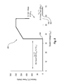
- FIG. 8 illustrates an example power/voltage curve 802 for the PV module 200 of FIG. 2 , arranged in accordance with at least some embodiments described herein.
- Example operation of the PV module 200 will now be described with combined reference to FIGS. 2-8 .
- the circuit card 610 including the digital controller 704 , is powered directly by the energy generated by the PV module 200 and not from an external supply. As such, the circuit card 610 is not powered in the absence of illumination, such as at night. Under sufficient illumination, the PV cells 404 generate sufficient voltage for the digital controller 704 to begin operating.
- the first operation performed by the digital controller 704 is to perform a series of checks to ensure safe module operation. For example, the digital controller 704 checks the voltage on the module-to-module bus by controlling the opto-relay 718 to measure the voltage on the module-to-module bus. If the voltage is above a maximum threshold 804 , the digital controller 704 does not allow energy to be output to the module-to module bus by causing the protection relay 716 to open or remain open (as previously mentioned, the protection relay 716 may default open). Instead, any energy generated by the PV cells 404 and received at the converters 702 may be shunted back into the PV cells 404 through the continuous backsheet 206 while the digital controller 704 continues monitoring the voltage on the module-to-module bus.
- the maximum threshold 804 is 60 volts in the example of FIG. 8 .
- the digital controller 704 controls the opto-relay 718 to trickle charge current from the output bus 726 to the module-to-module bus to determine whether a capacitive element is attached to the module-to-module bus. If the digital controller 704 determines that a capacitive element is attached to the module-to-module bus, the digital controller 704 continues to trickle charge current through the opto-relay 718 to the module-to-module bus until the voltage on the module-to-module bus rises above the minimum threshold 806 .
- a minimum threshold 806 such as 35 volts in the example of FIG. 8
- the digital controller 704 closes the protection relay 716 to ensure zero current switching.
- the digital controller 704 operates the converters 702 in a maximum current mode when the voltage on the module-to-module bus is between the minimum threshold 806 and an intermediate threshold 808 greater than the minimum threshold 806 .
- the intermediate threshold 808 is 57 volts in the example of FIG. 8 .
- the digital controller 704 operates the converters 702 in a constant voltage mode when the voltage on the module-to-module bus is between the intermediate threshold 808 and the maximum threshold 804 and opens the protection relay 716 when the voltage on the module-to-module bus rises above the maximum threshold 804 or falls below the minimum threshold 806 .
- the digital controller 704 charges up (e.g., operates) the converters 702 until the voltage on the output bus 726 matches the voltage on the module-to-module bus before closing the protection relay 716 to ensure zero current switching of the protection relay 716 .
- the digital controller 704 will then operate the converters 702 in maximum current mode or constant voltage mode, or will open the protection relay 716 , depending on the voltage on the module-to-module bus.
- the protection relay 716 enables a soft start control where the PV module 200 is isolated from the voltage on the module-to-module bus until one or more of the converters 702 are charged so that the voltage on the output bus 726 matches the voltage on the module-to-module bus before closing the protection relay 716 .
- the opto-relay 718 is a bypass circuit around the protection relay 716 that allows measurement of the external voltage on the module-to-module bus to ensure that the soft start is balanced, and to allow some small current to be fed into the module-to-module bus to assist in charging a capacitive element on the module-to-module bus in the event an energy storage device is not coupled thereto.
- each of the PV modules 200 operates independently of the others depending only on the voltage on the module-to-module bus as described herein, ensuring redundancy by eliminating dependencies on other PV modules 200 .
- Maximum current mode includes operating any number, from one to all, of the converters 702 so as to produce a maximum current output on the output bus 726 .
- the number of converters 702 operated at any given time depends on the amount of available current from the PV cells 404 , which is determined by changing PWM values of any single operating converter 702 and observing the resulting voltage change and power. If the voltage change is minimal and the power increases, a maximum peak power algorithm is executed, as described in more detail below. As the maximum peak power algorithm reaches optimum PWM values for the converters 702 , additional converters 702 may be enabled to continue taking (and outputting) more power. If the power decreases and the PWM values for the operating converters 702 fall below a threshold, one of the operating converters 702 may be disabled.
- the digital controller 704 may identify the failed converter 702 in memory. If the converter 702 fails short, the digital controller 704 may temporarily disable the other operating converters 702 and temporarily route all current through the failed converter 702 and its fuse 722 to open the fuse 722 as already explained above.
- FIG. 9 is a schematic diagram of an embodiment of one of the converters 702 of FIG. 7 , arranged in accordance with at least some embodiments described herein. Each of the converters 702 may be similarly configured.
- the converter 702 illustrated in FIG. 9 is merely one example of a converter that can be employed according to some embodiments and should not be construed to limit the invention in any way.
- the converter 702 includes an input 902 , a capacitor 904 coupled to the input 902 and to ground 906 , an inductor 908 coupled to the input 902 and to the capacitor 904 , a switch 910 coupled to the inductor 908 , a diode 912 coupled to the inductor 908 and to the switch 910 , an output 914 coupled to the diode 912 , a control line 916 coupled to the switch 910 , and one or more measurement circuits 918 coupled between the converter 702 and ground 906 .
- the input 902 is electrically coupled to the positive connector 706 through a corresponding fuse 722 .
- the ground 906 is electrically coupled to the continuous backsheet 206 through one of the negative connectors 708 and a corresponding one of the tabs 504 .
- the output 914 is electrically coupled to the output bus 726 .
- the control line 916 is communicatively coupled to the digital controller 704 and may correspond to one of the paired enable and PWM lines 724 .
- the digital controller 704 provides, via the control line 916 , a PWM signal to the switch 910 that controls the switching frequency and/or duty cycle of the converter 702 .
- the PWM signal controls the phasing of the converter 702 relative to the phasing of other converters 702 on the circuit card 610 .
- the switch 910 may include a field-effect transistor (“FET”), a metal-oxide-semiconductor FET (“MOSFET”), an insulated-gate bipolar transistor (“IGBT”), a bipolar junction transistor (“BJT”), or other suitable switch.
- FET field-effect transistor
- MOSFET metal-oxide-semiconductor FET
- IGBT insulated-gate bipolar transistor
- BJT bipolar junction transistor
- the diode 912 may include a Schottky rectifier, or other suitable diode.
- the measurement circuit 918 includes one or more resistors and is employed to measure certain operating parameters of the converter 702 .
- the measurement circuit 918 can measure the maximum current buildup per switching cycle in the inductor 908 in order to maintain maximum peak power.
- the measurement circuit 918 can measure the charging rate of the inductor 908 , the input voltage of the converter 702 , the output voltage of the converter 702 , or the like or any combination thereof.
- the converter 702 receives energy generated by any of the PV cells 404 at the input 902 and converts it to have a relatively higher voltage (referred to as the “step-up voltage”) and a lower current by switching itself on and off via the switch 910 .
- the switch 910 In the “on” state, the switch 910 is closed such that the current flowing through the inductor 908 increases and returns to ground 906 through the switch 910 and the measurement circuit 918 .
- the switch 910 In the “off” state, the switch 910 is open such that the current flowing through the inductor 908 decreases, flowing through the diode 912 and the output 914 to the output bus 726 .
- the voltage at the output 914 is about 0 volts.
- the voltage at the output 914 depends on the rate of change of current through the inductor 908 , rather than on the input voltage at the input 902 .
- the rate of change of current through the inductor 908 depends on the inductance of the inductor 908 .
- the step-up voltage at the output 914 depends on the inductance of the inductor 908 .
- the step-up voltage at the output 914 depends on the switching frequency of the switch 910 and/or the duty cycle of the switch 910 .
- the current through the inductor 908 never reaches 0 amps.
- the converter 702 produces conditioned power (e.g., power having the step-up voltage) at the output 914 while maximizing efficiency and minimizing peak current in the converter 702 .
- the converter 702 may be operated near continuous conduction mode by limiting the duty cycle D of the converter 702 to [(V_out ⁇ V_in)/V_out ⁇ 0.05] ⁇ D ⁇ 0.75, where V_out and V_in are the output voltage and the input voltage of the converter 702 and may be measured by the measurement circuit 918 .
- the switch 910 is operated via the control line 916 .
- the digital controller 704 sends signals over the control line 916 to open and close the switch 910 at a desired frequency and duty cycle. Because each of the step-up voltage and the impedance of the converter 702 depend on the frequency and the duty cycle of the switching process, the digital controller 704 can set the frequency and/or duty cycle at a predetermined frequency and/or duty cycle to optimize the step-up voltage and the impedance of the converter 702 .
- any individual converter 702 on the circuit card 610 may only be partially used in both duty cycle and frequency and may be part of a dynamic load-leveling cycle.
- the increasing and decreasing current through the inductor 908 can cause periodic variations in the amplitude of the input current and/or the output current of the converter 702 .
- These periodic variations in the current amplitude are also known as current ripple.
- Current ripple at the input 902 of the converter 702 can cause the impedance of the converter 702 to vary as a function of the current ripple, making it difficult for the converter 702 to maintain maximum peak power.
- Current ripple at the output of the converter 702 can result in noise on the output bus 726 that may negatively affect a load coupled to the output bus 726 .
- current ripple can be substantially reduced at the input and output of the circuit card 610 as a whole by operating the converters 702 out of phase with each other.
- the amplitude of current ripple in one of the converters 702 may be increasing while the amplitude of current ripple in another of the converters 702 may be decreasing.
- the cumulative effect of the out-of-phase operation of the converters 702 averages out the current ripple at the input and output of the circuit card 610 as a whole.
- maintaining peak power can maximize the unconditioned power output of the array of PV cells 404 , and consequently of the conditioned power output to the module-to-module bus.
- maintaining peak power includes (1) identifying a peak power point at which power output of the array of PV cells 404 is maximized and (2) dynamically varying the impedance of the converters 702 to effectively match the impedance of a load such that the voltage across the array of PV cells 404 is substantially equal to the identified peak power point.
- the load coupled to the module-to-module bus may be optimized to operate over a very narrow voltage range for maximum efficiency. Details of an example peak power algorithm are disclosed in more detail in U.S. patent application Ser. No. 12/357,260, filed Jan. 21, 2009, which application is herein incorporated by reference in its entirety.
- inventions described herein may include the use of a special purpose or general purpose computer, including various computer hardware or software modules, as discussed in greater detail below.
- Embodiments within the scope of the present invention also include computer-readable media for carrying or having computer-executable instructions or data structures stored thereon.
- Such computer-readable media can be any available media that can be accessed by a general purpose or special purpose computer.
- Such computer-readable media can include tangible computer-readable storage media including RAM, ROM, EEPROM, CD-ROM or other optical disk storage, magnetic disk storage or other magnetic storage devices, or any other storage medium which can be used to carry or store desired program code means in the form of computer-executable instructions or data structures and which can be accessed by a general purpose or special purpose computer. Combinations of the above should also be included within the scope of computer-readable media.
- Computer-executable instructions comprise, for example, instructions and data which cause a general purpose computer, special purpose computer, or special purpose processing device to perform a certain function or group of functions.
- module can refer to software objects or routines that execute on the computing system.
- the different components, modules, engines, and services described herein may be implemented as objects or processes that execute on the computing system (e.g., as separate threads). While the system and methods described herein are preferably implemented in software, implementations in hardware or a combination of software and hardware are also possible and contemplated.
- a “computing entity” may be any computing system as previously defined herein, or any module or combination of modulates running on a computing system.
Abstract
Description
- U.S. Provisional Application No. 61/553,822, filed Oct. 31, 2011, titled CONTINUOUS WIRE SOLAR PANEL CONNECTORS;
- U.S. Provisional Application No. 61/554,710, filed Nov. 2, 2011, titled PHASE BALANCING USING A SOLAR ARRAY OR A SOLAR/STORAGE ARRAY;
- U.S. Provisional Application No. 61/585,720, filed Jan. 12, 2012, titled MICRO-REPLICATION PATTERNS FOR SOLAR REFLECTORS;
- U.S. Provisional Application No. 61/590,925, filed Jan. 26, 2012, titled HIGHLY EFFICIENT SOLAR GREENHOUSE;
- U.S. Provisional Application No. 61/620,566, filed Apr. 5, 2012, titled REDUNDANT SOLAR MODULE AND SYSTEM;
- U.S. Provisional Application No. 61/694,548, filed Aug. 29, 2012, titled HIGHLY EFFICIENT, REDUNDANT LOW-VOLTAGE PHOTOVOLTAIC SOLAR TOPOLOGY;
- U.S. Provisional Application No. 61/694,559, filed Aug. 29, 2012, titled EFFECT OF PHOTOVOLTAIC MODULE SHADING PROPERTIES ON PROJECT ENERGY DENSITY; and
- U.S. Provisional Application No. 61/699,701, filed Sep. 11, 2012, titled CELL-TO-GRID REDUNDANT PHOTOVOLTAIC ARRAY.
Claims (30)
Priority Applications (2)
| Application Number | Priority Date | Filing Date | Title |
|---|---|---|---|
| US13/664,885 US9299861B2 (en) | 2010-06-15 | 2012-10-31 | Cell-to-grid redundandt photovoltaic system |
| US14/465,392 US20140360561A1 (en) | 2010-06-15 | 2014-08-21 | Fully redundant photovoltaic array |
Applications Claiming Priority (12)
| Application Number | Priority Date | Filing Date | Title |
|---|---|---|---|
| US12/815,913 US8563847B2 (en) | 2009-01-21 | 2010-06-15 | Illumination agnostic solar panel |
| US39286210P | 2010-10-13 | 2010-10-13 | |
| US13/207,164 US8829330B2 (en) | 2010-02-23 | 2011-08-10 | Highly efficient solar arrays |
| US201161553822P | 2011-10-31 | 2011-10-31 | |
| US201161554710P | 2011-11-02 | 2011-11-02 | |
| US201261585720P | 2012-01-12 | 2012-01-12 | |
| US201261590925P | 2012-01-26 | 2012-01-26 | |
| US201261620566P | 2012-04-05 | 2012-04-05 | |
| US201261694559P | 2012-08-29 | 2012-08-29 | |
| US201261694548P | 2012-08-29 | 2012-08-29 | |
| US201261699701P | 2012-09-11 | 2012-09-11 | |
| US13/664,885 US9299861B2 (en) | 2010-06-15 | 2012-10-31 | Cell-to-grid redundandt photovoltaic system |
Related Parent Applications (1)
| Application Number | Title | Priority Date | Filing Date |
|---|---|---|---|
| US12/815,913 Continuation-In-Part US8563847B2 (en) | 2009-01-21 | 2010-06-15 | Illumination agnostic solar panel |
Related Child Applications (1)
| Application Number | Title | Priority Date | Filing Date |
|---|---|---|---|
| US12/815,913 Continuation-In-Part US8563847B2 (en) | 2009-01-21 | 2010-06-15 | Illumination agnostic solar panel |
Publications (2)
| Publication Number | Publication Date |
|---|---|
| US20130062956A1 US20130062956A1 (en) | 2013-03-14 |
| US9299861B2 true US9299861B2 (en) | 2016-03-29 |
Family
ID=47829197
Family Applications (1)
| Application Number | Title | Priority Date | Filing Date |
|---|---|---|---|
| US13/664,885 Active 2032-02-18 US9299861B2 (en) | 2010-06-15 | 2012-10-31 | Cell-to-grid redundandt photovoltaic system |
Country Status (1)
| Country | Link |
|---|---|
| US (1) | US9299861B2 (en) |
Cited By (2)
| Publication number | Priority date | Publication date | Assignee | Title |
|---|---|---|---|---|
| US20150101761A1 (en) * | 2013-05-12 | 2015-04-16 | Solexel, Inc. | Solar photovoltaic blinds and curtains for residential and commercial buildings |
| CN109995087A (en) * | 2017-12-29 | 2019-07-09 | 北京天诚同创电气有限公司 | The frequency modulation control method, apparatus and frequency modulation system in power station |
Families Citing this family (12)
| Publication number | Priority date | Publication date | Assignee | Title |
|---|---|---|---|---|
| US8933320B2 (en) | 2008-01-18 | 2015-01-13 | Tenksolar, Inc. | Redundant electrical architecture for photovoltaic modules |
| US8748727B2 (en) * | 2008-01-18 | 2014-06-10 | Tenksolar, Inc. | Flat-plate photovoltaic module |
| US8212139B2 (en) | 2008-01-18 | 2012-07-03 | Tenksolar, Inc. | Thin-film photovoltaic module |
| IN2012DN00387A (en) | 2009-06-15 | 2015-08-21 | Tenksolar Inc | |
| US9773933B2 (en) | 2010-02-23 | 2017-09-26 | Tenksolar, Inc. | Space and energy efficient photovoltaic array |
| JP6019614B2 (en) * | 2012-02-28 | 2016-11-02 | オムロン株式会社 | Power storage control device, power storage control device control method, program, and power storage system |
| EP2770539A1 (en) * | 2013-02-20 | 2014-08-27 | Total Marketing Services | Electronic management system for electricity generating cells, electricity generating system and method for electronically managing energy flow |
| EP3036829A4 (en) * | 2013-08-21 | 2017-08-09 | Tenksolar, Inc. | Fully redundant photovoltaic array |
| US20150145336A1 (en) * | 2013-11-27 | 2015-05-28 | Solantro Semiconductor Corp. | Modular power conversion system and method |
| KR101631266B1 (en) * | 2014-11-28 | 2016-06-17 | (주)대은 | A Module of Abnormal Condition Diagnosis System in a serially connected photovoltaic module string and Method thereof |
| KR102589092B1 (en) * | 2018-11-05 | 2023-10-16 | 상라오 징코 솔라 테크놀러지 디벨롭먼트 컴퍼니, 리미티드 | Solar Cell Panel for Satellite |
| EP3683909B1 (en) * | 2019-01-15 | 2022-08-31 | Solaredge Technologies Ltd. | Safety switch for photovoltaic systems |
Citations (270)
| Publication number | Priority date | Publication date | Assignee | Title |
|---|---|---|---|---|
| US3094439A (en) | 1961-07-24 | 1963-06-18 | Spectrolab | Solar cell system |
| US3350234A (en) | 1963-06-03 | 1967-10-31 | Hoffman Electronics Corp | Flexible solar-cell concentrator array |
| US3419434A (en) | 1964-07-21 | 1968-12-31 | Martin Marietta Corp | Solar cell assemblies |
| US3833426A (en) | 1973-11-08 | 1974-09-03 | Trw Inc | Solar array |
| US4002160A (en) | 1975-02-12 | 1977-01-11 | Owens-Illinois, Inc. | Solar energy collection system |
| US4020827A (en) | 1975-08-20 | 1977-05-03 | Paul D. Harrigan | Solar energy collecting system |
| US4033327A (en) | 1975-11-24 | 1977-07-05 | Owens-Illinois, Inc. | Solar energy collector module system |
| US4120282A (en) | 1977-04-28 | 1978-10-17 | Espy Patrick N | Solar radiation reflector and collector array |
| US4154998A (en) | 1977-07-12 | 1979-05-15 | Trw Inc. | Solar array fabrication method and apparatus utilizing induction heating |
| US4158768A (en) | 1976-09-27 | 1979-06-19 | S.G.T.C. Societe Generale Internationale De Recherches Techniques Et De Consulence S.A. | Bi-axial scanning device for following the outline of a template |
| US4212293A (en) | 1978-04-07 | 1980-07-15 | Owens-Illinois, Inc. | Modular tubular solar energy collector apparatus |
| US4227298A (en) | 1978-09-05 | 1980-10-14 | Motorola, Inc. | Method for interconnecting photovoltaic devices |
| US4309334A (en) | 1975-10-08 | 1982-01-05 | Loctite Corporation | Thermally-resistant glass-filled adhesive/sealant compositions |
| US4316448A (en) | 1980-10-06 | 1982-02-23 | Pennwalt Corporation | Solar energy concentrator system |
| US4321416A (en) | 1980-12-15 | 1982-03-23 | Amp Incorporated | Photovoltaic power generation |
| US4369498A (en) | 1981-01-19 | 1983-01-18 | Texas Instruments Incorporated | Photoluminescent powered calculator |
| US4410757A (en) | 1982-03-22 | 1983-10-18 | Monegon, Ltd. | Adjustable collection members for solar energy systems |
| US4461922A (en) | 1983-02-14 | 1984-07-24 | Atlantic Richfield Company | Solar cell module |
| US4481378A (en) | 1982-07-30 | 1984-11-06 | Motorola, Inc. | Protected photovoltaic module |
| US4514579A (en) | 1984-01-30 | 1985-04-30 | Energy Conversion Devices, Inc. | Large area photovoltaic cell and method for producing same |
| JPS60141152U (en) | 1984-02-28 | 1985-09-18 | 株式会社東芝 | solar panel equipment |
| US4604494A (en) | 1984-11-07 | 1986-08-05 | General Electric Company | Photovoltaic cell array with light concentrating reflectors |
| US4611090A (en) | 1984-12-28 | 1986-09-09 | Standard Oil Company | Semirigid photovoltaic module assembly and structural support therefor |
| US4617421A (en) | 1985-04-01 | 1986-10-14 | Sovonics Solar Systems | Photovoltaic cell having increased active area and method for producing same |
| US4695788A (en) | 1984-12-11 | 1987-09-22 | Hughes Aircraft Company | Open fault location system for photovoltaic module strings |
| US4716258A (en) | 1987-01-23 | 1987-12-29 | Murtha R Michael | Stamped concentrators supporting photovoltaic assemblies |
| US4747699A (en) | 1985-02-06 | 1988-05-31 | Daikin Industries, Ltd. | Thermal-environment sensor with means to simulate emissivity of human body |
| US4755921A (en) | 1986-04-02 | 1988-07-05 | Minnesota Mining And Manufacturing Company | Lens |
| US4773944A (en) | 1987-09-08 | 1988-09-27 | Energy Conversion Devices, Inc. | Large area, low voltage, high current photovoltaic modules and method of fabricating same |
| DE3708548C2 (en) | 1987-03-17 | 1989-05-03 | Telefunken Electronic Gmbh, 7100 Heilbronn, De | |
| US4854974A (en) | 1987-06-29 | 1989-08-08 | Solarex Corporation | Electrical contacts for a thin-film semiconductor device |
| US4933022A (en) | 1988-11-14 | 1990-06-12 | Board Of Trustees Of The Leland Stanford Univ. & Electric Power Research Institute | Solar cell having interdigitated contacts and internal bypass diodes |
| JPH0225079Y2 (en) | 1985-08-30 | 1990-07-10 | ||
| US4964713A (en) | 1987-12-08 | 1990-10-23 | Fraunhofer-Gesellschaft zur Forderund der Forschung E. V. | Concentrator arrangement |
| US4966631A (en) | 1989-03-13 | 1990-10-30 | Chronar Corp. | Support for photovoltaic arrays |
| US5013141A (en) | 1985-02-21 | 1991-05-07 | Canon Kabushiki Kaisha | Liquid crystal light modulation device |
| US5021099A (en) | 1988-08-09 | 1991-06-04 | The Boeing Company | Solar cell interconnection and packaging using tape carrier |
| US5048194A (en) | 1987-12-05 | 1991-09-17 | Renishaw Plc | Position sensing probe |
| US5096505A (en) | 1990-05-21 | 1992-03-17 | The Boeing Company | Panel for solar concentrators and tandem cell units |
| DE4027325A1 (en) | 1990-08-29 | 1992-04-02 | Siemens Ag | Solar cell assembly with rigid field of straight current conductors - has regular division of conductor pairs via feeds of flexibly suspended single solar cells |
| US5205739A (en) | 1989-11-13 | 1993-04-27 | Augat Inc. | High density parallel interconnect |
| US5246782A (en) | 1990-12-10 | 1993-09-21 | The Dow Chemical Company | Laminates of polymers having perfluorocyclobutane rings and polymers containing perfluorocyclobutane rings |
| US5268037A (en) | 1992-05-21 | 1993-12-07 | United Solar Systems Corporation | Monolithic, parallel connected photovoltaic array and method for its manufacture |
| US5270636A (en) | 1992-02-18 | 1993-12-14 | Lafferty Donald L | Regulating control circuit for photovoltaic source employing switches, energy storage, and pulse width modulation controller |
| US5288337A (en) | 1992-06-25 | 1994-02-22 | Siemens Solar Industries, L.P. | Photovoltaic module with specular reflector |
| US5344497A (en) | 1993-04-19 | 1994-09-06 | Fraas Lewis M | Line-focus photovoltaic module using stacked tandem-cells |
| US5374317A (en) | 1990-09-26 | 1994-12-20 | Energy Systems Solar, Incorporated | Multiple reflector concentrator solar electric power system |
| US5457057A (en) | 1994-06-28 | 1995-10-10 | United Solar Systems Corporation | Photovoltaic module fabrication process |
| US5468988A (en) | 1994-03-04 | 1995-11-21 | United Solar Systems Corporation | Large area, through-hole, parallel-connected photovoltaic device |
| US5478402A (en) | 1994-02-17 | 1995-12-26 | Ase Americas, Inc. | Solar cell modules and method of making same |
| US5491040A (en) | 1993-06-08 | 1996-02-13 | Chaloner-Gill; Benjamin | Dual purpose lithium salt for electrochemical cells |
| US5493096A (en) | 1994-05-10 | 1996-02-20 | Grumman Aerospace Corporation | Thin substrate micro-via interconnect |
| US5505789A (en) | 1993-04-19 | 1996-04-09 | Entech, Inc. | Line-focus photovoltaic module using solid optical secondaries for improved radiation resistance |
| US5513075A (en) | 1992-05-08 | 1996-04-30 | The Whitaker Corporation | Module for electrically connecting conductor wires to circuits of flat surfaces such as solar panels |
| US5538563A (en) | 1995-02-03 | 1996-07-23 | Finkl; Anthony W. | Solar energy concentrator apparatus for bifacial photovoltaic cells |
| US5571338A (en) | 1993-11-26 | 1996-11-05 | Sanyo Electric Co., Ltd. | Photovoltaic module and a photovoltaic apparatus |
| US5593901A (en) | 1989-09-08 | 1997-01-14 | Amoco/Enron Solar | Monolithic series and parallel connected photovoltaic module |
| JPH0945946A (en) | 1995-07-31 | 1997-02-14 | Sanyo Electric Co Ltd | Solar cell and fabrication thereof |
| US5719758A (en) | 1995-12-20 | 1998-02-17 | Sharp Kabushiki Kaisha | Inverter control method and inverter apparatus using the method |
| JPH1069321A (en) | 1996-08-27 | 1998-03-10 | Honda Motor Co Ltd | Photovoltaic power device |
| US5735966A (en) | 1995-05-15 | 1998-04-07 | Luch; Daniel | Substrate structures for integrated series connected photovoltaic arrays and process of manufacture of such arrays |
| US5745355A (en) | 1996-06-25 | 1998-04-28 | Exide Electronics Corporation | Wireless selective tripping of AC power systems connected in parallel |
| US5801519A (en) | 1996-06-21 | 1998-09-01 | The Board Of Trustees Of The University Of Illinois | Self-excited power minimizer/maximizer for switching power converters and switching motor drive applications |
| JPH10245935A (en) | 1997-03-07 | 1998-09-14 | Ykk Architect Prod Kk | Building panel with solar battery |
| JPH10281562A (en) | 1997-04-07 | 1998-10-23 | Sekisui Chem Co Ltd | Opto-thermo hybrid panel and its method of manufacture |
| KR19980087002A (en) | 1997-05-14 | 1998-12-05 | 미따라이 후지오 | Photovoltaic power generation apparatus |
| JPH1141832A (en) | 1997-07-17 | 1999-02-12 | Nippon Telegr & Teleph Corp <Ntt> | System and method for solar cell generation |
| JPH11103538A (en) | 1997-09-27 | 1999-04-13 | My Way Giken Kk | Optical power generating system |
| US5896281A (en) | 1997-07-02 | 1999-04-20 | Raytheon Company | Power conditioning system for a four quadrant photovoltaic array with an inverter for each array quadrant |
| US5910738A (en) | 1995-04-07 | 1999-06-08 | Kabushiki Kaisha Toshiba | Driving circuit for driving a semiconductor device at high speed and method of operating the same |
| US5982157A (en) | 1997-02-17 | 1999-11-09 | Asulab S.A. | Chopper-amplifier for the voltage of a photovoltaic power source, in particular for a timepiece |
| US5990413A (en) | 1996-06-19 | 1999-11-23 | Ortabasi; Ugur | Bifacial lightweight array for solar power |
| US5994641A (en) | 1998-04-24 | 1999-11-30 | Ase Americas, Inc. | Solar module having reflector between cells |
| US6011215A (en) | 1997-12-18 | 2000-01-04 | United Solar Systems Corporation | Point contact photovoltaic module and method for its manufacture |
| US6017002A (en) | 1997-07-21 | 2000-01-25 | Hughes Electronics Corporation | Thin-film solar reflectors deployable from an edge-stowed configuration |
| US6043425A (en) | 1998-10-02 | 2000-03-28 | Hughes Electronics Corporation | Solar power source with textured solar concentrator |
| US6077722A (en) | 1998-07-14 | 2000-06-20 | Bp Solarex | Producing thin film photovoltaic modules with high integrity interconnects and dual layer contacts |
| JP2000213255A (en) | 1999-01-26 | 2000-08-02 | Kajima Corp | Light shelf used also as solar battery |
| US6111767A (en) | 1998-06-22 | 2000-08-29 | Heliotronics, Inc. | Inverter integrated instrumentation having a current-voltage curve tracer |
| US6111189A (en) | 1998-07-28 | 2000-08-29 | Bp Solarex | Photovoltaic module framing system with integral electrical raceways |
| US6134784A (en) | 1999-08-27 | 2000-10-24 | Photovoltaics International, Llc | Method of making solar collectors by in-situ encapsulation of solar cells |
| JP2000357812A (en) | 1999-04-15 | 2000-12-26 | Canon Inc | Solar battery module and generation device |
| US6177627B1 (en) | 1999-06-21 | 2001-01-23 | Ace-Able Engineering Co., Inc. | Solar cell array with multiple rows of cells and collapsible reflectors |
| US6188012B1 (en) | 1999-11-10 | 2001-02-13 | Tecstar Power Systems | Methods and systems for a solar cell concentrator |
| US6201180B1 (en) | 1999-04-16 | 2001-03-13 | Omnion Power Engineering Corp. | Integrated photovoltaic system |
| US20010008144A1 (en) | 1998-02-26 | 2001-07-19 | Tsuyoshi Uematsu | Photovoltalic device, photovoltaic module and establishing method of photovoltaic system |
| US6281485B1 (en) | 2000-09-27 | 2001-08-28 | The Aerospace Corporation | Maximum power tracking solar power system |
| JP2001268891A (en) | 2000-03-22 | 2001-09-28 | Kanegafuchi Chem Ind Co Ltd | Power unit using solar cell |
| US6331208B1 (en) | 1998-05-15 | 2001-12-18 | Canon Kabushiki Kaisha | Process for producing solar cell, process for producing thin-film semiconductor, process for separating thin-film semiconductor, and process for forming semiconductor |
| US6337436B1 (en) | 1999-05-07 | 2002-01-08 | Webasto Vehicle Systems International Gmbh | Solar module for attachment to motor vehicles and a process for its manufacture |
| GB2331530B (en) | 1997-11-15 | 2002-01-23 | Brian Paget | A decking system for floors and other surface areas |
| US6351130B1 (en) | 1998-06-26 | 2002-02-26 | Fraunhofer-Gesellschaft Zur Foerderung Der Angewandten Foschung E.V. | Device for testing solar home systems |
| JP2002073184A (en) | 2000-08-31 | 2002-03-12 | Matsushita Electric Works Ltd | Photovoltaic power generation system |
| US20020038667A1 (en) * | 2000-09-29 | 2002-04-04 | Hiroshi Kondo | Solar battery module and power generation apparatus |
| WO2002035613A1 (en) | 2000-10-20 | 2002-05-02 | Josuke Nakata | Light-emitting or light-detecting semiconductor module and method of manufacture thereof |
| US6462265B1 (en) | 1995-08-15 | 2002-10-08 | Canon Kabushiki Kaisha | Terminal lead-out structure and solar-cell apparatus provided with such structure |
| JP2002305318A (en) | 2001-04-05 | 2002-10-18 | Mitsubishi Heavy Ind Ltd | Photovoltaic power generation system |
| JP2002314112A (en) | 2001-04-16 | 2002-10-25 | Sumitomo 3M Ltd | Photovoltaic power generating system |
| US6479744B1 (en) | 1997-12-22 | 2002-11-12 | Canon Kabushiki Kaisha | Photovoltaic device module |
| US20020179140A1 (en) | 2001-05-30 | 2002-12-05 | Fumitaka Toyomura | Power converter, and photovoltaic element module and power generator using the same |
| JP2003026455A (en) | 2001-07-13 | 2003-01-29 | Sharp Corp | Solar battery module |
| US6515215B1 (en) | 1998-03-13 | 2003-02-04 | Canon Kabushiki Kaisha | Photovoltaic module, photovoltaic module array, photovoltaic system, and method of detecting failure of photovoltaic module |
| US6528716B2 (en) | 2000-07-20 | 2003-03-04 | Universite De Liege | Solar concentrator |
| US20030047208A1 (en) | 2001-09-11 | 2003-03-13 | The Boeing Company | Low cost high solar flux photovoltaic concentrator receiver |
| US20030121542A1 (en) | 2000-03-30 | 2003-07-03 | Wolfgang Harneit | Method for producing a solar module with thin-film solar cells which are series-connected in an integrated manner and solar modules produced according to the method, especially using concentrator modules |
| US20030121228A1 (en) | 2001-12-31 | 2003-07-03 | Stoehr Robert P. | System and method for dendritic web solar cell shingling |
| JP2003282918A (en) | 2002-03-27 | 2003-10-03 | Sanko Seiki Kk | Mobile solar cell generating set |
| US20030201007A1 (en) | 2002-04-24 | 2003-10-30 | Fraas Lewis M. | Planar solar concentrator power module |
| DE20314372U1 (en) | 2002-12-23 | 2003-12-04 | Day4 Energy Inc. | Solar energy concentrator for solar energy system has reflector made up of many plane facets approximating parabolic mirror, focusing sunlight on array of photovoltaic cells |
| US20040016454A1 (en) | 1999-06-21 | 2004-01-29 | Aec-Able Engineering Co., Inc. | Solar cell array |
| WO2004021455A1 (en) | 2002-08-29 | 2004-03-11 | Day4 Energy Inc. | Electrode for photovoltaic cells, photovoltaic cell and photovoltaic module |
| US6706963B2 (en) | 2002-01-25 | 2004-03-16 | Konarka Technologies, Inc. | Photovoltaic cell interconnection |
| US20040055594A1 (en) | 2002-09-20 | 2004-03-25 | Hochberg Eric B. | Lightweight, low-cost solar energy collector |
| US20040089337A1 (en) | 2002-11-09 | 2004-05-13 | Tao-Hung Chou | Circuit device for solar energy application |
| US6739692B2 (en) | 2001-05-10 | 2004-05-25 | Canon Kabushiki Kaisha | Ink jet recording apparatus |
| US6750391B2 (en) | 2001-10-25 | 2004-06-15 | Sandia Corporation | Aternating current photovoltaic building block |
| US6753692B2 (en) | 2000-03-29 | 2004-06-22 | Canon Kabushiki Kaisha | Method and apparatus for testing solar panel, manufacturing method for manufacturing the solar panel, method and apparatus for inspecting solar panel generating system, insulation resistance measuring apparatus, and withstand voltage tester |
| US6803513B2 (en) | 2002-08-20 | 2004-10-12 | United Solar Systems Corporation | Series connected photovoltaic module and method for its manufacture |
| US20040261955A1 (en) | 2003-03-10 | 2004-12-30 | Powerlight Corporation | Modular shade system |
| US20040261834A1 (en) | 2001-08-23 | 2004-12-30 | Basore Paul A | Chain link metal interconnect structure |
| DE102004001248B3 (en) | 2004-01-07 | 2005-01-05 | Day4 Energy Inc. | Stationary photovoltaic solar energy concentrator has light reception surfaces of photovoltaic receivers positioned in focal planes of lens elements of non-imaging Fresnel lens |
| US20050000562A1 (en) | 2003-04-10 | 2005-01-06 | Canon Kabushiki Kaisha | Solar cell module having an electric device |
| US20050022857A1 (en) | 2003-08-01 | 2005-02-03 | Daroczi Shandor G. | Solar cell interconnect structure |
| US20050034751A1 (en) | 2003-07-10 | 2005-02-17 | William Gross | Solar concentrator array with individually adjustable elements |
| US6858461B2 (en) | 2000-07-06 | 2005-02-22 | Bp Corporation North America Inc. | Partially transparent photovoltaic modules |
| US6870087B1 (en) | 2001-09-14 | 2005-03-22 | Patrick Gallagher | Assembly method and apparatus for photovoltaic module |
| US20050061360A1 (en) | 2001-10-12 | 2005-03-24 | Tatsuji Horioka | Photovoltaic solar cell module assembly, wiring system and photovoltaic power system |
| US6882063B2 (en) | 2000-07-28 | 2005-04-19 | International Power Systems, Inc. | DC to DC converter and power management system |
| US20050081909A1 (en) | 2003-10-20 | 2005-04-21 | Paull James B. | Concentrating solar roofing shingle |
| US20050115176A1 (en) | 2002-04-11 | 2005-06-02 | Rwe Schott Solar, Inc. | Apparatus and method for mounting photovoltaic power generating systems on buildings |
| US6903261B2 (en) | 2001-05-23 | 2005-06-07 | Universite De Liege | Solar concentrator |
| US20050121067A1 (en) | 2002-07-09 | 2005-06-09 | Canon Kabushiki Kaisha | Solar power generation apparatus, solar power generation system, and method of manufacturing solar power generation apparatus |
| CN1628390A (en) | 2002-06-21 | 2005-06-15 | 中田仗祐 | Light-emitting device and its prodn. method |
| US20050133081A1 (en) | 2003-11-25 | 2005-06-23 | Ixys Corporation | Photo voltaic solar cells integrated with mosfet |
| US20050158891A1 (en) | 2000-05-30 | 2005-07-21 | Barth Kurt L. | Apparatus and processes for the mass production of photovoltaic modules |
| US20050172995A1 (en) | 2002-05-17 | 2005-08-11 | Rudiger Rohrig | Circuit arrangement for a photovoltaic system |
| US20050194939A1 (en) | 2000-01-04 | 2005-09-08 | Duff William B.Jr. | Method and circuit for using polarized device in AC applications |
| US6966184B2 (en) | 2002-11-25 | 2005-11-22 | Canon Kabushiki Kaisha | Photovoltaic power generating apparatus, method of producing same and photovoltaic power generating system |
| US20050263179A1 (en) | 2004-06-01 | 2005-12-01 | Russell Gaudiana | Photovoltaic module architecture |
| US20050268959A1 (en) | 2004-06-04 | 2005-12-08 | Sunpower Corporation | Interconnection of solar cells in a solar cell module |
| US20050278076A1 (en) | 2003-07-17 | 2005-12-15 | Frano Barbir | Method and apparatus for operating and controlling a power system |
| US20060001406A1 (en) | 2004-07-01 | 2006-01-05 | Stefan Matan | Power extractor circuit |
| US6992256B1 (en) | 2005-08-01 | 2006-01-31 | Wiley Electronics Llc | External disconnect mechanism integrated with an electrical system enclosure |
| JP2006040931A (en) | 2004-07-22 | 2006-02-09 | Nagano Japan Radio Co | Apparatus for generating solar light power |
| US20060042681A1 (en) | 2004-08-24 | 2006-03-02 | General Electric Company | Pv laminate backplane with optical concentrator |
| US7009412B2 (en) | 1999-05-27 | 2006-03-07 | Nanonexus, Inc. | Massively parallel interface for electronic circuit |
| US20060054212A1 (en) | 2004-09-10 | 2006-03-16 | Fraas Lewis M | Solar photovoltaic mirror modules |
| US20060092588A1 (en) | 2004-10-28 | 2006-05-04 | Realmuto Richard A | Multiple bi-directional input/output power control system |
| US20060162772A1 (en) | 2005-01-18 | 2006-07-27 | Presher Gordon E Jr | System and method for monitoring photovoltaic power generation systems |
| US20060174931A1 (en) | 2001-11-16 | 2006-08-10 | First Solar, Llc A Delaware Corporation | Photovoltaic array |
| US20060174939A1 (en) | 2004-12-29 | 2006-08-10 | Isg Technologies Llc | Efficiency booster circuit and technique for maximizing power point tracking |
| US20060180197A1 (en) | 2005-02-15 | 2006-08-17 | Gui John Y | Layer-to-layer interconnects for photoelectric devices and methods of fabricating the same |
| US7094441B2 (en) | 2002-01-25 | 2006-08-22 | Konarka Technologies, Inc. | Low temperature interconnection of nanoparticles |
| US20060185727A1 (en) | 2004-12-29 | 2006-08-24 | Isg Technologies Llc | Converter circuit and technique for increasing the output efficiency of a variable power source |
| US20060185716A1 (en) | 2005-02-18 | 2006-08-24 | Clean Venture 21 Corporation | Method for producing photovoltaic device and photovoltaic device |
| US7099169B2 (en) | 2003-02-21 | 2006-08-29 | Distributed Power, Inc. | DC to AC inverter with single-switch bipolar boost circuit |
| US20060213548A1 (en) | 2005-03-22 | 2006-09-28 | Applied Materials, Inc. | Scalable photovoltaic cell and solar panel manufacturing with improved wiring |
| US20060225777A1 (en) | 2005-04-11 | 2006-10-12 | Unaxis Balzers Ltd. | Solar cell module and method of encapsulating same |
| US20060235717A1 (en) | 2005-04-18 | 2006-10-19 | Solaria Corporation | Method and system for manufacturing solar panels using an integrated solar cell using a plurality of photovoltaic regions |
| JP2006302147A (en) | 2005-04-22 | 2006-11-02 | Nippon Telegr & Teleph Corp <Ntt> | Booster |
| US7138730B2 (en) | 2002-11-22 | 2006-11-21 | Virginia Tech Intellectual Properties, Inc. | Topologies for multiple energy sources |
| EP1724842A2 (en) | 2005-05-18 | 2006-11-22 | Goldbeck Solar GmbH | Lining for a surface, in particular for the surface of a building |
| US20060261830A1 (en) | 2005-04-07 | 2006-11-23 | Bill Taylor | Inverter thermal protection |
| US20060266407A1 (en) | 2005-03-10 | 2006-11-30 | Lichy Joseph I | Apparatus and method for electrically connecting photovoltaic cells in a photovoltaic device |
| US20070035864A1 (en) | 2001-12-17 | 2007-02-15 | Vasylyev Sergiy V | Multistage system for radiant energy flux transformation |
| US20070056626A1 (en) | 2005-09-12 | 2007-03-15 | Solaria Corporation | Method and system for assembling a solar cell using a plurality of photovoltaic regions |
| US20070068567A1 (en) | 2005-09-23 | 2007-03-29 | Rubin Leonid B | Testing apparatus and method for solar cells |
| US20070079861A1 (en) | 2003-11-12 | 2007-04-12 | Anthony Morali | Solar rail or railing system |
| US20070095384A1 (en) | 2005-10-28 | 2007-05-03 | Farquhar Donald S | Photovoltaic modules and interconnect methodology for fabricating the same |
| US20070103108A1 (en) | 2003-05-28 | 2007-05-10 | Beacon Power Corporation | Power converter for a solar panel |
| US20070113885A1 (en) | 2005-08-15 | 2007-05-24 | Chan Randolph W | Photovoltaic cells with interconnects to external circuit |
| US20070124619A1 (en) | 2005-11-25 | 2007-05-31 | Satoshi Mizukami | Power supply system |
| US20070125415A1 (en) | 2005-12-05 | 2007-06-07 | Massachusetts Institute Of Technology | Light capture with patterned solar cell bus wires |
| WO2007071064A1 (en) | 2005-12-23 | 2007-06-28 | Day4 Energy Inc. | Solar cell with physically separated distributed electrical contacts |
| US20070151594A1 (en) | 2005-12-29 | 2007-07-05 | Powerlight Corporation | One Piece, Collapsible PV Assembly |
| US20070157964A1 (en) | 2006-01-09 | 2007-07-12 | Solyndra, Inc. | Interconnects for solar cell devices |
| US20070179720A1 (en) | 2006-01-27 | 2007-08-02 | Sma Technologie Ag | Method for converting direct voltage into three-phase alternating voltage |
| US20070186971A1 (en) | 2005-01-20 | 2007-08-16 | Nanosolar, Inc. | High-efficiency solar cell with insulated vias |
| US20070193620A1 (en) | 2006-01-17 | 2007-08-23 | Hines Braden E | Concentrating solar panel and related systems and methods |
| WO2007095757A1 (en) | 2006-02-24 | 2007-08-30 | Day4 Energy Inc. | High voltage solar cell and solar cell module |
| JP2007234795A (en) | 2006-02-28 | 2007-09-13 | Sharp Corp | Solar battery module, solar battery module string, solar battery array, solar power generation system, and power cable |
| US20070215195A1 (en) | 2006-03-18 | 2007-09-20 | Benyamin Buller | Elongated photovoltaic cells in tubular casings |
| US7276724B2 (en) | 2005-01-20 | 2007-10-02 | Nanosolar, Inc. | Series interconnected optoelectronic device module assembly |
| US20070235077A1 (en) | 2006-03-27 | 2007-10-11 | Kyocera Corporation | Solar Cell Module and Manufacturing Process Thereof |
| US20070240755A1 (en) | 2006-03-22 | 2007-10-18 | Nuedison Corporation | Apparatus and method for construction and placement of a non-equatorial photovoltaic module |
| KR20070104300A (en) | 2007-06-20 | 2007-10-25 | 황우성 | Concentrating photovoltaic module structure |
| US20070251569A1 (en) | 2006-01-25 | 2007-11-01 | Intematix Corporation | Solar modules with tracking and concentrating features |
| KR20070107318A (en) | 2006-05-02 | 2007-11-07 | 윤종호 | Solar cell module structure |
| JP2007294630A (en) | 2006-04-25 | 2007-11-08 | Msk Corp | Solar cell generator |
| US20070261731A1 (en) | 2004-09-03 | 2007-11-15 | Shin-Etsu Chemical Co., Ltd., | Photovoltaic Power Generation Module and Photovoltaic Power Generation System Employing Same |
| US7297865B2 (en) | 2003-08-01 | 2007-11-20 | Sunpower Corporation | Compact micro-concentrator for photovoltaic cells |
| US20070266672A1 (en) | 2006-05-19 | 2007-11-22 | Solar Century Holdings Limited | Solar panel roof mounting system |
| US20070273338A1 (en) | 2006-05-23 | 2007-11-29 | Distributed Power, Inc. | Transformerless Utility-Grid-Interactive Inverter |
| US20070272295A1 (en) | 2006-05-26 | 2007-11-29 | Rubin Leonid B | Heat sink for photovoltaic cells |
| DE202006020180U1 (en) | 2006-09-08 | 2007-12-27 | Koller, Alexander, Dipl.-Ing. | solar roof |
| US20070295381A1 (en) | 2004-03-29 | 2007-12-27 | Kyocera Corporation | Solar Cell Module and Photovoltaic Power Generator Using This |
| US20080000516A1 (en) | 2004-09-14 | 2008-01-03 | Aerosun Technologies Ag | Solar Energy Utilization Unit and Solar Energy Utilization System |
| US20080029149A1 (en) | 2006-08-02 | 2008-02-07 | Daniel Simon | Method and apparatus for arranging a solar cell and reflector |
| US20080029152A1 (en) | 2006-08-04 | 2008-02-07 | Erel Milshtein | Laser scribing apparatus, systems, and methods |
| WO2008016453A2 (en) | 2006-08-02 | 2008-02-07 | Daniel Simon | Method and apparatus for arranging a solar cell and reflector |
| US20080037141A1 (en) | 2006-08-11 | 2008-02-14 | Sol Focus, Inc. | Method for alignment of optical elements in an array |
| US7339108B2 (en) | 2002-01-07 | 2008-03-04 | Thales | Solar energy concentrator device for spacecraft and a solar generator panel |
| US7342171B2 (en) | 2003-01-23 | 2008-03-11 | Solar Intergrated Technologies, Inc. | Integrated photovoltaic roofing component and panel |
| WO2008042828A2 (en) | 2006-10-02 | 2008-04-10 | Johnson & Johnson Consumer Companies, Inc. | Imaging apparatus and methods for capturing and analyzing digital images of the skin |
| WO2008046201A1 (en) | 2006-10-16 | 2008-04-24 | Day4 Energy Inc. | Semiconductor structure and process for forming ohmic connections to a semiconductor structure |
| US20080111517A1 (en) * | 2006-11-15 | 2008-05-15 | Pfeifer John E | Charge Controller for DC-DC Power Conversion |
| US20080122518A1 (en) | 2006-11-27 | 2008-05-29 | Besser David A | Multi-Source, Multi-Load Systems with a Power Extractor |
| US20080142071A1 (en) | 2006-12-15 | 2008-06-19 | Miasole | Protovoltaic module utilizing a flex circuit for reconfiguration |
| US20080163922A1 (en) | 2007-01-08 | 2008-07-10 | Horne William E | Conversion of solar energy to electrical and/or heat energy |
| US20080164766A1 (en) | 2006-12-06 | 2008-07-10 | Meir Adest | Current bypass for distributed power harvesting systems using dc power sources |
| US20080210286A1 (en) | 2007-03-01 | 2008-09-04 | Ball Newton E | Parallel and virtual parallel interconnection of solar cells in solar panels |
| US20080236648A1 (en) | 2007-03-30 | 2008-10-02 | Klein David L | Localized power point optimizer for solar cell installations |
| US20080290368A1 (en) | 2007-05-21 | 2008-11-27 | Day4 Energy, Inc. | Photovoltaic cell with shallow emitter |
| WO2008141415A1 (en) | 2007-05-17 | 2008-11-27 | Day4 Energy Inc. | Photovoltaic cell with shallow emitter |
| US20080298051A1 (en) | 2007-05-29 | 2008-12-04 | Ko-Chien Chu | Flat-plate lighting device |
| JP2009503870A (en) | 2005-07-26 | 2009-01-29 | ソラリア コーポレーション | Solar panel manufacturing method and system using integrated solar cells including a plurality of photovoltaic regions |
| US20090025778A1 (en) | 2007-07-23 | 2009-01-29 | Day4 Energy Inc. | Shading protection for solar cells and solar cell modules |
| JP2009032945A (en) | 2007-07-27 | 2009-02-12 | Sharp Corp | Photovoltaic generation system |
| US20090121968A1 (en) | 2007-11-08 | 2009-05-14 | Murata Machinery, Ltd. | Electronic Device |
| US20090151775A1 (en) | 2007-12-17 | 2009-06-18 | Solar Integrated Technologies Gmbh | System for Assisting Solar Power Generation |
| WO2009076740A1 (en) | 2007-12-18 | 2009-06-25 | Day4 Energy Inc. | Photovoltaic module with edge access to pv strings, interconnection method, apparatus, and system |
| US20090183763A1 (en) | 2008-01-18 | 2009-07-23 | Tenksolar, Inc | Flat-Plate Photovoltaic Module |
| US20090183760A1 (en) | 2008-01-18 | 2009-07-23 | Tenksolar Inc | Redundant electrical architecture for photovoltaic modules |
| US20090183764A1 (en) | 2008-01-18 | 2009-07-23 | Tenksolar, Inc | Detachable Louver System |
| WO2009092110A2 (en) | 2008-01-18 | 2009-07-23 | Tenksolar, Inc. | Redundant electrical architecture for photovoltaic modules |
| US20090217965A1 (en) | 2006-04-21 | 2009-09-03 | Dougal Roger A | Apparatus and method for enhanced solar power generation and maximum power point tracking |
| US20090242021A1 (en) | 2008-03-31 | 2009-10-01 | Noribachi Llc | Solar cell with colorization layer |
| US20090250093A1 (en) | 2008-04-08 | 2009-10-08 | Zupei Chen | Enhanced concentrator PV pannel |
| WO2009092111A3 (en) | 2008-01-18 | 2009-11-19 | Tenksolar, Inc. | Flat-plate photovoltaic module |
| US20090296348A1 (en) * | 2008-05-20 | 2009-12-03 | Miles Clayton Russell | Ac photovoltaic module and inverter assembly |
| US20100014738A1 (en) | 2008-07-21 | 2010-01-21 | Tomtec Imaging Systems Gmbh | Method and system for breast cancer screening |
| EP2172980A1 (en) | 2007-07-10 | 2010-04-07 | José Javier Alejo Trevijano | Solar energy concentrator and assembly method |
| WO2010037393A1 (en) | 2008-10-01 | 2010-04-08 | Sunsil A/S | Power generation system and method of operating a power generation system |
| US20100089390A1 (en) | 2008-10-13 | 2010-04-15 | Sunlink, Corp | Solar array mounting system |
| US20100101624A1 (en) * | 2007-06-20 | 2010-04-29 | Emanuela Fioretti | Photovoltaic module and modular panel made with it to collect radiant solar energy |
| US20100131108A1 (en) | 2008-01-18 | 2010-05-27 | Tenksolar, Inc | Thin-film photovoltaic module |
| WO2010068226A1 (en) | 2008-12-12 | 2010-06-17 | Paceco Corp. | System for controlling power from a photovoltaic array by selectively configuring connections between photovoltaic panels |
| US20100175337A1 (en) | 2009-01-13 | 2010-07-15 | Optisolar Inc. | Flexible roof-mount system and method for solar panels |
| US20100206378A1 (en) * | 2009-02-13 | 2010-08-19 | Miasole | Thin-film photovoltaic power system with integrated low-profile high-efficiency inverter |
| WO2010096833A2 (en) | 2009-02-23 | 2010-08-26 | Tenksolar, Inc. | Highly efficient renewable energy system |
| US20100219688A1 (en) | 2008-07-17 | 2010-09-02 | Atomic Energy Council-Institute Of Nuclear Energy Research | DC Power System for Household Appliances |
| US20100253151A1 (en) | 2009-04-01 | 2010-10-07 | Gerhardinger Peter F | Grid tie solar system and a method |
| US20100282293A1 (en) | 2009-01-21 | 2010-11-11 | Tenksolar | Illumination agnostic solar panel |
| EP2251941A1 (en) | 2009-05-15 | 2010-11-17 | Femtogrid Energy Solutions B.V. | A DC wall outlet/inlet with controlled connect and disconnect sequence to limit arcing |
| JP2010263027A (en) | 2009-05-01 | 2010-11-18 | Onamba Co Ltd | Apparatus for detecting abnormality of solar cell power generation system and method therefor |
| TW201042770A (en) | 2009-05-26 | 2010-12-01 | Day4 Energy Inc | Photovoltaic module string arrangement and shading protection therefor |
| KR20100129721A (en) | 2007-12-21 | 2010-12-09 | 심파기스 테크놀로지, 인크. | Advanced renewable energy harvesting |
| US20100313499A1 (en) | 2009-06-10 | 2010-12-16 | Gangemi Ronald J | Roof mounting bracket for photovoltaic power generation system |
| US20100313933A1 (en) | 2008-02-21 | 2010-12-16 | Jianguo Xu | Reflector-solar receiver assembly and solar module |
| JP2011002991A (en) | 2009-06-18 | 2011-01-06 | Nissan Motor Co Ltd | Power supply device |
| US20110018353A1 (en) | 2009-07-23 | 2011-01-27 | Wenjiang Yu | Method and apparatus for multi-source electrical energy grid-tied transformation |
| WO2011011855A1 (en) | 2009-07-31 | 2011-02-03 | Day4 Energy Inc. | Method for interconnecting back contact solar cells and photovoltaic module employing same |
| TW201106490A (en) | 2009-08-12 | 2011-02-16 | Day4 Energy Inc | Method for interconnecting back contact solar cells and photovoltaic module employing same |
| US20110039992A1 (en) | 2006-12-27 | 2011-02-17 | Masakazu Irie | Method of Improving Stability Of Organopolysiloxane And An Organopolysiloxane Mixture |
| US20110067748A1 (en) | 2009-09-18 | 2011-03-24 | Inventux Technologies Ag | Solar system |
| WO2010012062A8 (en) | 2008-07-28 | 2011-04-28 | Day4 Energy Inc. | Crystalline silicon pv cell with selective emitter produced with low temperature precision etch back and passivation process |
| JP2011129626A (en) | 2009-12-16 | 2011-06-30 | Gf Giken:Kk | Reflected light utilization type solar light module system |
| US20110175662A1 (en) * | 2010-01-19 | 2011-07-21 | General Electric Company | Open circuit voltage protection system and method |
| US7997938B2 (en) | 2009-10-22 | 2011-08-16 | Tyco Electronics Corporation | Electrical connector system with electrical power connection and guide features |
| US20110199040A1 (en) * | 2010-02-12 | 2011-08-18 | Suncore, Inc. | Stand alone solar battery charger |
| WO2011109741A1 (en) | 2010-03-05 | 2011-09-09 | Elq Energy, Inc. | Low cost pcb carrier and connectivity system for enclosed electronics |
| US20110241431A1 (en) | 2010-04-01 | 2011-10-06 | Daoshen Chen | Solar light power generation system, control device, and control method thereof |
| US20110301772A1 (en) | 2010-06-07 | 2011-12-08 | Zuercher Joseph C | Protection, monitoring or indication apparatus for a direct current electrical generating apparatus or a plurality of strings |
| US20120042588A1 (en) | 2009-05-11 | 2012-02-23 | The Regents Of The University Of Colorado | Integrated photovoltaic module |
| US20120204935A1 (en) | 2010-02-23 | 2012-08-16 | Tenksolar | Highly efficient solar arrays |
| US20120215372A1 (en) * | 2008-12-15 | 2012-08-23 | Array Converter Inc. | Detection and Prevention of Hot Spots in a Solar Panel |
| US20120319494A1 (en) | 2011-06-15 | 2012-12-20 | Schneider Electric Industries Sas | Secure control mechanism for distributed photovoltaic system |
| EP1744372A3 (en) | 2005-07-13 | 2013-01-16 | Zeta Controls Limited | Solar panel |
| US20130312812A1 (en) | 2010-02-23 | 2013-11-28 | Tenksolar, Inc | Space and energy efficient photovoltaic array |
| US20140360561A1 (en) | 2010-06-15 | 2014-12-11 | Tenksolar, Inc. | Fully redundant photovoltaic array |
-
2012
- 2012-10-31 US US13/664,885 patent/US9299861B2/en active Active
Patent Citations (309)
| Publication number | Priority date | Publication date | Assignee | Title |
|---|---|---|---|---|
| US3094439A (en) | 1961-07-24 | 1963-06-18 | Spectrolab | Solar cell system |
| US3350234A (en) | 1963-06-03 | 1967-10-31 | Hoffman Electronics Corp | Flexible solar-cell concentrator array |
| US3419434A (en) | 1964-07-21 | 1968-12-31 | Martin Marietta Corp | Solar cell assemblies |
| US3833426A (en) | 1973-11-08 | 1974-09-03 | Trw Inc | Solar array |
| US4002160A (en) | 1975-02-12 | 1977-01-11 | Owens-Illinois, Inc. | Solar energy collection system |
| US4020827A (en) | 1975-08-20 | 1977-05-03 | Paul D. Harrigan | Solar energy collecting system |
| US4309334A (en) | 1975-10-08 | 1982-01-05 | Loctite Corporation | Thermally-resistant glass-filled adhesive/sealant compositions |
| US4033327A (en) | 1975-11-24 | 1977-07-05 | Owens-Illinois, Inc. | Solar energy collector module system |
| US4158768A (en) | 1976-09-27 | 1979-06-19 | S.G.T.C. Societe Generale Internationale De Recherches Techniques Et De Consulence S.A. | Bi-axial scanning device for following the outline of a template |
| US4120282A (en) | 1977-04-28 | 1978-10-17 | Espy Patrick N | Solar radiation reflector and collector array |
| US4154998A (en) | 1977-07-12 | 1979-05-15 | Trw Inc. | Solar array fabrication method and apparatus utilizing induction heating |
| US4212293A (en) | 1978-04-07 | 1980-07-15 | Owens-Illinois, Inc. | Modular tubular solar energy collector apparatus |
| US4227298A (en) | 1978-09-05 | 1980-10-14 | Motorola, Inc. | Method for interconnecting photovoltaic devices |
| US4316448A (en) | 1980-10-06 | 1982-02-23 | Pennwalt Corporation | Solar energy concentrator system |
| US4321416A (en) | 1980-12-15 | 1982-03-23 | Amp Incorporated | Photovoltaic power generation |
| US4369498A (en) | 1981-01-19 | 1983-01-18 | Texas Instruments Incorporated | Photoluminescent powered calculator |
| US4410757A (en) | 1982-03-22 | 1983-10-18 | Monegon, Ltd. | Adjustable collection members for solar energy systems |
| US4481378A (en) | 1982-07-30 | 1984-11-06 | Motorola, Inc. | Protected photovoltaic module |
| US4461922A (en) | 1983-02-14 | 1984-07-24 | Atlantic Richfield Company | Solar cell module |
| US4514579A (en) | 1984-01-30 | 1985-04-30 | Energy Conversion Devices, Inc. | Large area photovoltaic cell and method for producing same |
| JPS60141152U (en) | 1984-02-28 | 1985-09-18 | 株式会社東芝 | solar panel equipment |
| US4604494A (en) | 1984-11-07 | 1986-08-05 | General Electric Company | Photovoltaic cell array with light concentrating reflectors |
| US4695788A (en) | 1984-12-11 | 1987-09-22 | Hughes Aircraft Company | Open fault location system for photovoltaic module strings |
| US4611090A (en) | 1984-12-28 | 1986-09-09 | Standard Oil Company | Semirigid photovoltaic module assembly and structural support therefor |
| US4747699A (en) | 1985-02-06 | 1988-05-31 | Daikin Industries, Ltd. | Thermal-environment sensor with means to simulate emissivity of human body |
| US5013141A (en) | 1985-02-21 | 1991-05-07 | Canon Kabushiki Kaisha | Liquid crystal light modulation device |
| US4617421A (en) | 1985-04-01 | 1986-10-14 | Sovonics Solar Systems | Photovoltaic cell having increased active area and method for producing same |
| JPH0225079Y2 (en) | 1985-08-30 | 1990-07-10 | ||
| US4755921A (en) | 1986-04-02 | 1988-07-05 | Minnesota Mining And Manufacturing Company | Lens |
| US4716258A (en) | 1987-01-23 | 1987-12-29 | Murtha R Michael | Stamped concentrators supporting photovoltaic assemblies |
| DE3708548C2 (en) | 1987-03-17 | 1989-05-03 | Telefunken Electronic Gmbh, 7100 Heilbronn, De | |
| US4854974A (en) | 1987-06-29 | 1989-08-08 | Solarex Corporation | Electrical contacts for a thin-film semiconductor device |
| US4773944A (en) | 1987-09-08 | 1988-09-27 | Energy Conversion Devices, Inc. | Large area, low voltage, high current photovoltaic modules and method of fabricating same |
| US5048194A (en) | 1987-12-05 | 1991-09-17 | Renishaw Plc | Position sensing probe |
| US4964713A (en) | 1987-12-08 | 1990-10-23 | Fraunhofer-Gesellschaft zur Forderund der Forschung E. V. | Concentrator arrangement |
| US5021099A (en) | 1988-08-09 | 1991-06-04 | The Boeing Company | Solar cell interconnection and packaging using tape carrier |
| US4933022A (en) | 1988-11-14 | 1990-06-12 | Board Of Trustees Of The Leland Stanford Univ. & Electric Power Research Institute | Solar cell having interdigitated contacts and internal bypass diodes |
| US4966631A (en) | 1989-03-13 | 1990-10-30 | Chronar Corp. | Support for photovoltaic arrays |
| US5593901A (en) | 1989-09-08 | 1997-01-14 | Amoco/Enron Solar | Monolithic series and parallel connected photovoltaic module |
| US5205739A (en) | 1989-11-13 | 1993-04-27 | Augat Inc. | High density parallel interconnect |
| US5096505A (en) | 1990-05-21 | 1992-03-17 | The Boeing Company | Panel for solar concentrators and tandem cell units |
| DE4027325A1 (en) | 1990-08-29 | 1992-04-02 | Siemens Ag | Solar cell assembly with rigid field of straight current conductors - has regular division of conductor pairs via feeds of flexibly suspended single solar cells |
| US5374317A (en) | 1990-09-26 | 1994-12-20 | Energy Systems Solar, Incorporated | Multiple reflector concentrator solar electric power system |
| US5246782A (en) | 1990-12-10 | 1993-09-21 | The Dow Chemical Company | Laminates of polymers having perfluorocyclobutane rings and polymers containing perfluorocyclobutane rings |
| US5270636A (en) | 1992-02-18 | 1993-12-14 | Lafferty Donald L | Regulating control circuit for photovoltaic source employing switches, energy storage, and pulse width modulation controller |
| US5513075A (en) | 1992-05-08 | 1996-04-30 | The Whitaker Corporation | Module for electrically connecting conductor wires to circuits of flat surfaces such as solar panels |
| US5268037A (en) | 1992-05-21 | 1993-12-07 | United Solar Systems Corporation | Monolithic, parallel connected photovoltaic array and method for its manufacture |
| US5288337A (en) | 1992-06-25 | 1994-02-22 | Siemens Solar Industries, L.P. | Photovoltaic module with specular reflector |
| US5344497A (en) | 1993-04-19 | 1994-09-06 | Fraas Lewis M | Line-focus photovoltaic module using stacked tandem-cells |
| US5505789A (en) | 1993-04-19 | 1996-04-09 | Entech, Inc. | Line-focus photovoltaic module using solid optical secondaries for improved radiation resistance |
| US5491040A (en) | 1993-06-08 | 1996-02-13 | Chaloner-Gill; Benjamin | Dual purpose lithium salt for electrochemical cells |
| US5571338A (en) | 1993-11-26 | 1996-11-05 | Sanyo Electric Co., Ltd. | Photovoltaic module and a photovoltaic apparatus |
| US5478402A (en) | 1994-02-17 | 1995-12-26 | Ase Americas, Inc. | Solar cell modules and method of making same |
| US5468988A (en) | 1994-03-04 | 1995-11-21 | United Solar Systems Corporation | Large area, through-hole, parallel-connected photovoltaic device |
| US5493096A (en) | 1994-05-10 | 1996-02-20 | Grumman Aerospace Corporation | Thin substrate micro-via interconnect |
| US5457057A (en) | 1994-06-28 | 1995-10-10 | United Solar Systems Corporation | Photovoltaic module fabrication process |
| US5538563A (en) | 1995-02-03 | 1996-07-23 | Finkl; Anthony W. | Solar energy concentrator apparatus for bifacial photovoltaic cells |
| US6111454A (en) | 1995-04-07 | 2000-08-29 | Kabushiki Kaisha Toshiba | Power supply circuit |
| US5910738A (en) | 1995-04-07 | 1999-06-08 | Kabushiki Kaisha Toshiba | Driving circuit for driving a semiconductor device at high speed and method of operating the same |
| US5735966A (en) | 1995-05-15 | 1998-04-07 | Luch; Daniel | Substrate structures for integrated series connected photovoltaic arrays and process of manufacture of such arrays |
| JPH0945946A (en) | 1995-07-31 | 1997-02-14 | Sanyo Electric Co Ltd | Solar cell and fabrication thereof |
| US6462265B1 (en) | 1995-08-15 | 2002-10-08 | Canon Kabushiki Kaisha | Terminal lead-out structure and solar-cell apparatus provided with such structure |
| US5719758A (en) | 1995-12-20 | 1998-02-17 | Sharp Kabushiki Kaisha | Inverter control method and inverter apparatus using the method |
| US5990413A (en) | 1996-06-19 | 1999-11-23 | Ortabasi; Ugur | Bifacial lightweight array for solar power |
| US5801519A (en) | 1996-06-21 | 1998-09-01 | The Board Of Trustees Of The University Of Illinois | Self-excited power minimizer/maximizer for switching power converters and switching motor drive applications |
| US5745355A (en) | 1996-06-25 | 1998-04-28 | Exide Electronics Corporation | Wireless selective tripping of AC power systems connected in parallel |
| JPH1069321A (en) | 1996-08-27 | 1998-03-10 | Honda Motor Co Ltd | Photovoltaic power device |
| US5982157A (en) | 1997-02-17 | 1999-11-09 | Asulab S.A. | Chopper-amplifier for the voltage of a photovoltaic power source, in particular for a timepiece |
| JPH10245935A (en) | 1997-03-07 | 1998-09-14 | Ykk Architect Prod Kk | Building panel with solar battery |
| JPH10281562A (en) | 1997-04-07 | 1998-10-23 | Sekisui Chem Co Ltd | Opto-thermo hybrid panel and its method of manufacture |
| KR19980087002A (en) | 1997-05-14 | 1998-12-05 | 미따라이 후지오 | Photovoltaic power generation apparatus |
| US5896281A (en) | 1997-07-02 | 1999-04-20 | Raytheon Company | Power conditioning system for a four quadrant photovoltaic array with an inverter for each array quadrant |
| JPH1141832A (en) | 1997-07-17 | 1999-02-12 | Nippon Telegr & Teleph Corp <Ntt> | System and method for solar cell generation |
| US6017002A (en) | 1997-07-21 | 2000-01-25 | Hughes Electronics Corporation | Thin-film solar reflectors deployable from an edge-stowed configuration |
| JPH11103538A (en) | 1997-09-27 | 1999-04-13 | My Way Giken Kk | Optical power generating system |
| GB2331530B (en) | 1997-11-15 | 2002-01-23 | Brian Paget | A decking system for floors and other surface areas |
| US6011215A (en) | 1997-12-18 | 2000-01-04 | United Solar Systems Corporation | Point contact photovoltaic module and method for its manufacture |
| US6479744B1 (en) | 1997-12-22 | 2002-11-12 | Canon Kabushiki Kaisha | Photovoltaic device module |
| US20010008144A1 (en) | 1998-02-26 | 2001-07-19 | Tsuyoshi Uematsu | Photovoltalic device, photovoltaic module and establishing method of photovoltaic system |
| US6294723B2 (en) | 1998-02-26 | 2001-09-25 | Hitachi, Ltd. | Photovoltaic device, photovoltaic module and establishing method of photovoltaic system |
| US6515215B1 (en) | 1998-03-13 | 2003-02-04 | Canon Kabushiki Kaisha | Photovoltaic module, photovoltaic module array, photovoltaic system, and method of detecting failure of photovoltaic module |
| US5994641A (en) | 1998-04-24 | 1999-11-30 | Ase Americas, Inc. | Solar module having reflector between cells |
| US6331208B1 (en) | 1998-05-15 | 2001-12-18 | Canon Kabushiki Kaisha | Process for producing solar cell, process for producing thin-film semiconductor, process for separating thin-film semiconductor, and process for forming semiconductor |
| US6339538B1 (en) | 1998-06-22 | 2002-01-15 | Clayton Kling Philips Handleman | Inverter circuit and method of operation |
| US6111767A (en) | 1998-06-22 | 2000-08-29 | Heliotronics, Inc. | Inverter integrated instrumentation having a current-voltage curve tracer |
| US6351130B1 (en) | 1998-06-26 | 2002-02-26 | Fraunhofer-Gesellschaft Zur Foerderung Der Angewandten Foschung E.V. | Device for testing solar home systems |
| US6288325B1 (en) | 1998-07-14 | 2001-09-11 | Bp Corporation North America Inc. | Producing thin film photovoltaic modules with high integrity interconnects and dual layer contacts |
| US6077722A (en) | 1998-07-14 | 2000-06-20 | Bp Solarex | Producing thin film photovoltaic modules with high integrity interconnects and dual layer contacts |
| US6111189A (en) | 1998-07-28 | 2000-08-29 | Bp Solarex | Photovoltaic module framing system with integral electrical raceways |
| US6465724B1 (en) | 1998-07-28 | 2002-10-15 | Bp Solar International Llc | Photovoltaic module framing system with integral electrical raceways |
| JP2000114571A (en) | 1998-10-02 | 2000-04-21 | Hughes Electronics Corp | Solar battery power source having woven solar light converging device |
| US6043425A (en) | 1998-10-02 | 2000-03-28 | Hughes Electronics Corporation | Solar power source with textured solar concentrator |
| JP2000213255A (en) | 1999-01-26 | 2000-08-02 | Kajima Corp | Light shelf used also as solar battery |
| JP2000357812A (en) | 1999-04-15 | 2000-12-26 | Canon Inc | Solar battery module and generation device |
| US6201180B1 (en) | 1999-04-16 | 2001-03-13 | Omnion Power Engineering Corp. | Integrated photovoltaic system |
| US6337436B1 (en) | 1999-05-07 | 2002-01-08 | Webasto Vehicle Systems International Gmbh | Solar module for attachment to motor vehicles and a process for its manufacture |
| US7009412B2 (en) | 1999-05-27 | 2006-03-07 | Nanonexus, Inc. | Massively parallel interface for electronic circuit |
| US6177627B1 (en) | 1999-06-21 | 2001-01-23 | Ace-Able Engineering Co., Inc. | Solar cell array with multiple rows of cells and collapsible reflectors |
| US7301095B2 (en) | 1999-06-21 | 2007-11-27 | Aec-Able Engineering Co., Inc. | Solar cell array |
| US20040016454A1 (en) | 1999-06-21 | 2004-01-29 | Aec-Able Engineering Co., Inc. | Solar cell array |
| US6134784A (en) | 1999-08-27 | 2000-10-24 | Photovoltaics International, Llc | Method of making solar collectors by in-situ encapsulation of solar cells |
| US6188012B1 (en) | 1999-11-10 | 2001-02-13 | Tecstar Power Systems | Methods and systems for a solar cell concentrator |
| US20050194939A1 (en) | 2000-01-04 | 2005-09-08 | Duff William B.Jr. | Method and circuit for using polarized device in AC applications |
| JP2001268891A (en) | 2000-03-22 | 2001-09-28 | Kanegafuchi Chem Ind Co Ltd | Power unit using solar cell |
| US6753692B2 (en) | 2000-03-29 | 2004-06-22 | Canon Kabushiki Kaisha | Method and apparatus for testing solar panel, manufacturing method for manufacturing the solar panel, method and apparatus for inspecting solar panel generating system, insulation resistance measuring apparatus, and withstand voltage tester |
| US20030121542A1 (en) | 2000-03-30 | 2003-07-03 | Wolfgang Harneit | Method for producing a solar module with thin-film solar cells which are series-connected in an integrated manner and solar modules produced according to the method, especially using concentrator modules |
| US20050158891A1 (en) | 2000-05-30 | 2005-07-21 | Barth Kurt L. | Apparatus and processes for the mass production of photovoltaic modules |
| US6858461B2 (en) | 2000-07-06 | 2005-02-22 | Bp Corporation North America Inc. | Partially transparent photovoltaic modules |
| US6528716B2 (en) | 2000-07-20 | 2003-03-04 | Universite De Liege | Solar concentrator |
| US6882063B2 (en) | 2000-07-28 | 2005-04-19 | International Power Systems, Inc. | DC to DC converter and power management system |
| JP2002073184A (en) | 2000-08-31 | 2002-03-12 | Matsushita Electric Works Ltd | Photovoltaic power generation system |
| US6281485B1 (en) | 2000-09-27 | 2001-08-28 | The Aerospace Corporation | Maximum power tracking solar power system |
| US20020038667A1 (en) * | 2000-09-29 | 2002-04-04 | Hiroshi Kondo | Solar battery module and power generation apparatus |
| US7205626B1 (en) | 2000-10-20 | 2007-04-17 | Josuke Nakata | Light-emitting or light-receiving with plurality of particle-shaped semiconductor devices having light-emitting or light-receiving properties |
| WO2002035613A1 (en) | 2000-10-20 | 2002-05-02 | Josuke Nakata | Light-emitting or light-detecting semiconductor module and method of manufacture thereof |
| JP2002305318A (en) | 2001-04-05 | 2002-10-18 | Mitsubishi Heavy Ind Ltd | Photovoltaic power generation system |
| JP2002314112A (en) | 2001-04-16 | 2002-10-25 | Sumitomo 3M Ltd | Photovoltaic power generating system |
| US6739692B2 (en) | 2001-05-10 | 2004-05-25 | Canon Kabushiki Kaisha | Ink jet recording apparatus |
| US6903261B2 (en) | 2001-05-23 | 2005-06-07 | Universite De Liege | Solar concentrator |
| US20020179140A1 (en) | 2001-05-30 | 2002-12-05 | Fumitaka Toyomura | Power converter, and photovoltaic element module and power generator using the same |
| CN1388636A (en) | 2001-05-30 | 2003-01-01 | 佳能株式会社 | Power converter, photovoltaic element assembly and power generation equipment using the same assembly |
| JP2003026455A (en) | 2001-07-13 | 2003-01-29 | Sharp Corp | Solar battery module |
| US20040261834A1 (en) | 2001-08-23 | 2004-12-30 | Basore Paul A | Chain link metal interconnect structure |
| US20030047208A1 (en) | 2001-09-11 | 2003-03-13 | The Boeing Company | Low cost high solar flux photovoltaic concentrator receiver |
| US6870087B1 (en) | 2001-09-14 | 2005-03-22 | Patrick Gallagher | Assembly method and apparatus for photovoltaic module |
| US20050061360A1 (en) | 2001-10-12 | 2005-03-24 | Tatsuji Horioka | Photovoltaic solar cell module assembly, wiring system and photovoltaic power system |
| US6750391B2 (en) | 2001-10-25 | 2004-06-15 | Sandia Corporation | Aternating current photovoltaic building block |
| US20060174931A1 (en) | 2001-11-16 | 2006-08-10 | First Solar, Llc A Delaware Corporation | Photovoltaic array |
| US20070035864A1 (en) | 2001-12-17 | 2007-02-15 | Vasylyev Sergiy V | Multistage system for radiant energy flux transformation |
| US20030121228A1 (en) | 2001-12-31 | 2003-07-03 | Stoehr Robert P. | System and method for dendritic web solar cell shingling |
| US7339108B2 (en) | 2002-01-07 | 2008-03-04 | Thales | Solar energy concentrator device for spacecraft and a solar generator panel |
| US7094441B2 (en) | 2002-01-25 | 2006-08-22 | Konarka Technologies, Inc. | Low temperature interconnection of nanoparticles |
| US6706963B2 (en) | 2002-01-25 | 2004-03-16 | Konarka Technologies, Inc. | Photovoltaic cell interconnection |
| JP2003282918A (en) | 2002-03-27 | 2003-10-03 | Sanko Seiki Kk | Mobile solar cell generating set |
| US20050115176A1 (en) | 2002-04-11 | 2005-06-02 | Rwe Schott Solar, Inc. | Apparatus and method for mounting photovoltaic power generating systems on buildings |
| US20030201007A1 (en) | 2002-04-24 | 2003-10-30 | Fraas Lewis M. | Planar solar concentrator power module |
| US7388146B2 (en) | 2002-04-24 | 2008-06-17 | Jx Crystals Inc. | Planar solar concentrator power module |
| US20050172995A1 (en) | 2002-05-17 | 2005-08-11 | Rudiger Rohrig | Circuit arrangement for a photovoltaic system |
| CN1628390A (en) | 2002-06-21 | 2005-06-15 | 中田仗祐 | Light-emitting device and its prodn. method |
| US20060086384A1 (en) | 2002-06-21 | 2006-04-27 | Josuke Nakata | Light receiving or light emitting device and itsd production method |
| US20050121067A1 (en) | 2002-07-09 | 2005-06-09 | Canon Kabushiki Kaisha | Solar power generation apparatus, solar power generation system, and method of manufacturing solar power generation apparatus |
| US6803513B2 (en) | 2002-08-20 | 2004-10-12 | United Solar Systems Corporation | Series connected photovoltaic module and method for its manufacture |
| US7432438B2 (en) | 2002-08-29 | 2008-10-07 | Day 4 Energy Inc. | Electrode for photovoltaic cells, photovoltaic cell and photovoltaic module |
| WO2004021455A1 (en) | 2002-08-29 | 2004-03-11 | Day4 Energy Inc. | Electrode for photovoltaic cells, photovoltaic cell and photovoltaic module |
| US8013239B2 (en) | 2002-08-29 | 2011-09-06 | Day4 Energy Inc. | Electrode for photovoltaic cells, photovoltaic cell and photovoltaic module |
| US20040055594A1 (en) | 2002-09-20 | 2004-03-25 | Hochberg Eric B. | Lightweight, low-cost solar energy collector |
| US20040089337A1 (en) | 2002-11-09 | 2004-05-13 | Tao-Hung Chou | Circuit device for solar energy application |
| US7336004B2 (en) | 2002-11-22 | 2008-02-26 | Siemens Vdo Automotive Corporation | Topologies for using multiple energy sources for power conversions |
| US7138730B2 (en) | 2002-11-22 | 2006-11-21 | Virginia Tech Intellectual Properties, Inc. | Topologies for multiple energy sources |
| US6966184B2 (en) | 2002-11-25 | 2005-11-22 | Canon Kabushiki Kaisha | Photovoltaic power generating apparatus, method of producing same and photovoltaic power generating system |
| DE20314372U1 (en) | 2002-12-23 | 2003-12-04 | Day4 Energy Inc. | Solar energy concentrator for solar energy system has reflector made up of many plane facets approximating parabolic mirror, focusing sunlight on array of photovoltaic cells |
| US7342171B2 (en) | 2003-01-23 | 2008-03-11 | Solar Intergrated Technologies, Inc. | Integrated photovoltaic roofing component and panel |
| US7099169B2 (en) | 2003-02-21 | 2006-08-29 | Distributed Power, Inc. | DC to AC inverter with single-switch bipolar boost circuit |
| US20040261955A1 (en) | 2003-03-10 | 2004-12-30 | Powerlight Corporation | Modular shade system |
| US20050000562A1 (en) | 2003-04-10 | 2005-01-06 | Canon Kabushiki Kaisha | Solar cell module having an electric device |
| US20070103108A1 (en) | 2003-05-28 | 2007-05-10 | Beacon Power Corporation | Power converter for a solar panel |
| US20050034751A1 (en) | 2003-07-10 | 2005-02-17 | William Gross | Solar concentrator array with individually adjustable elements |
| US20050278076A1 (en) | 2003-07-17 | 2005-12-15 | Frano Barbir | Method and apparatus for operating and controlling a power system |
| US7297865B2 (en) | 2003-08-01 | 2007-11-20 | Sunpower Corporation | Compact micro-concentrator for photovoltaic cells |
| US20050022857A1 (en) | 2003-08-01 | 2005-02-03 | Daroczi Shandor G. | Solar cell interconnect structure |
| US20050081909A1 (en) | 2003-10-20 | 2005-04-21 | Paull James B. | Concentrating solar roofing shingle |
| US20070079861A1 (en) | 2003-11-12 | 2007-04-12 | Anthony Morali | Solar rail or railing system |
| US20050133081A1 (en) | 2003-11-25 | 2005-06-23 | Ixys Corporation | Photo voltaic solar cells integrated with mosfet |
| DE102004001248B3 (en) | 2004-01-07 | 2005-01-05 | Day4 Energy Inc. | Stationary photovoltaic solar energy concentrator has light reception surfaces of photovoltaic receivers positioned in focal planes of lens elements of non-imaging Fresnel lens |
| US20070295381A1 (en) | 2004-03-29 | 2007-12-27 | Kyocera Corporation | Solar Cell Module and Photovoltaic Power Generator Using This |
| US20050263179A1 (en) | 2004-06-01 | 2005-12-01 | Russell Gaudiana | Photovoltaic module architecture |
| US20050268959A1 (en) | 2004-06-04 | 2005-12-08 | Sunpower Corporation | Interconnection of solar cells in a solar cell module |
| US20060001406A1 (en) | 2004-07-01 | 2006-01-05 | Stefan Matan | Power extractor circuit |
| JP2006040931A (en) | 2004-07-22 | 2006-02-09 | Nagano Japan Radio Co | Apparatus for generating solar light power |
| US20060042681A1 (en) | 2004-08-24 | 2006-03-02 | General Electric Company | Pv laminate backplane with optical concentrator |
| US20070261731A1 (en) | 2004-09-03 | 2007-11-15 | Shin-Etsu Chemical Co., Ltd., | Photovoltaic Power Generation Module and Photovoltaic Power Generation System Employing Same |
| US20060054212A1 (en) | 2004-09-10 | 2006-03-16 | Fraas Lewis M | Solar photovoltaic mirror modules |
| US20080000516A1 (en) | 2004-09-14 | 2008-01-03 | Aerosun Technologies Ag | Solar Energy Utilization Unit and Solar Energy Utilization System |
| US20060092588A1 (en) | 2004-10-28 | 2006-05-04 | Realmuto Richard A | Multiple bi-directional input/output power control system |
| US20060185727A1 (en) | 2004-12-29 | 2006-08-24 | Isg Technologies Llc | Converter circuit and technique for increasing the output efficiency of a variable power source |
| US20060174939A1 (en) | 2004-12-29 | 2006-08-10 | Isg Technologies Llc | Efficiency booster circuit and technique for maximizing power point tracking |
| US20060162772A1 (en) | 2005-01-18 | 2006-07-27 | Presher Gordon E Jr | System and method for monitoring photovoltaic power generation systems |
| US20070186971A1 (en) | 2005-01-20 | 2007-08-16 | Nanosolar, Inc. | High-efficiency solar cell with insulated vias |
| US7276724B2 (en) | 2005-01-20 | 2007-10-02 | Nanosolar, Inc. | Series interconnected optoelectronic device module assembly |
| US20060180197A1 (en) | 2005-02-15 | 2006-08-17 | Gui John Y | Layer-to-layer interconnects for photoelectric devices and methods of fabricating the same |
| US20060185716A1 (en) | 2005-02-18 | 2006-08-24 | Clean Venture 21 Corporation | Method for producing photovoltaic device and photovoltaic device |
| US20060266407A1 (en) | 2005-03-10 | 2006-11-30 | Lichy Joseph I | Apparatus and method for electrically connecting photovoltaic cells in a photovoltaic device |
| US20060213548A1 (en) | 2005-03-22 | 2006-09-28 | Applied Materials, Inc. | Scalable photovoltaic cell and solar panel manufacturing with improved wiring |
| US20060261830A1 (en) | 2005-04-07 | 2006-11-23 | Bill Taylor | Inverter thermal protection |
| US20060225777A1 (en) | 2005-04-11 | 2006-10-12 | Unaxis Balzers Ltd. | Solar cell module and method of encapsulating same |
| US20060235717A1 (en) | 2005-04-18 | 2006-10-19 | Solaria Corporation | Method and system for manufacturing solar panels using an integrated solar cell using a plurality of photovoltaic regions |
| JP2006302147A (en) | 2005-04-22 | 2006-11-02 | Nippon Telegr & Teleph Corp <Ntt> | Booster |
| EP1724842A2 (en) | 2005-05-18 | 2006-11-22 | Goldbeck Solar GmbH | Lining for a surface, in particular for the surface of a building |
| EP1744372A3 (en) | 2005-07-13 | 2013-01-16 | Zeta Controls Limited | Solar panel |
| JP2009503870A (en) | 2005-07-26 | 2009-01-29 | ソラリア コーポレーション | Solar panel manufacturing method and system using integrated solar cells including a plurality of photovoltaic regions |
| US6992256B1 (en) | 2005-08-01 | 2006-01-31 | Wiley Electronics Llc | External disconnect mechanism integrated with an electrical system enclosure |
| US20070113885A1 (en) | 2005-08-15 | 2007-05-24 | Chan Randolph W | Photovoltaic cells with interconnects to external circuit |
| US20070056626A1 (en) | 2005-09-12 | 2007-03-15 | Solaria Corporation | Method and system for assembling a solar cell using a plurality of photovoltaic regions |
| US20070068567A1 (en) | 2005-09-23 | 2007-03-29 | Rubin Leonid B | Testing apparatus and method for solar cells |
| US20070095384A1 (en) | 2005-10-28 | 2007-05-03 | Farquhar Donald S | Photovoltaic modules and interconnect methodology for fabricating the same |
| US20070124619A1 (en) | 2005-11-25 | 2007-05-31 | Satoshi Mizukami | Power supply system |
| US20070125415A1 (en) | 2005-12-05 | 2007-06-07 | Massachusetts Institute Of Technology | Light capture with patterned solar cell bus wires |
| US20070144577A1 (en) | 2005-12-23 | 2007-06-28 | Rubin George L | Solar cell with physically separated distributed electrical contacts |
| WO2007071064A1 (en) | 2005-12-23 | 2007-06-28 | Day4 Energy Inc. | Solar cell with physically separated distributed electrical contacts |
| US20070151594A1 (en) | 2005-12-29 | 2007-07-05 | Powerlight Corporation | One Piece, Collapsible PV Assembly |
| CN101336476A (en) | 2005-12-29 | 2008-12-31 | 尚能系统有限公司 | One piece, collapsible pv assembly |
| US20070157964A1 (en) | 2006-01-09 | 2007-07-12 | Solyndra, Inc. | Interconnects for solar cell devices |
| US7259322B2 (en) | 2006-01-09 | 2007-08-21 | Solyndra, Inc. | Interconnects for solar cell devices |
| US20070193620A1 (en) | 2006-01-17 | 2007-08-23 | Hines Braden E | Concentrating solar panel and related systems and methods |
| US20070251569A1 (en) | 2006-01-25 | 2007-11-01 | Intematix Corporation | Solar modules with tracking and concentrating features |
| US20070179720A1 (en) | 2006-01-27 | 2007-08-02 | Sma Technologie Ag | Method for converting direct voltage into three-phase alternating voltage |
| US7498508B2 (en) | 2006-02-24 | 2009-03-03 | Day4 Energy, Inc. | High voltage solar cell and solar cell module |
| US20070199588A1 (en) | 2006-02-24 | 2007-08-30 | Rubin Leonid B | High voltage solar cell and solar cell module |
| WO2007095757A1 (en) | 2006-02-24 | 2007-08-30 | Day4 Energy Inc. | High voltage solar cell and solar cell module |
| JP2007234795A (en) | 2006-02-28 | 2007-09-13 | Sharp Corp | Solar battery module, solar battery module string, solar battery array, solar power generation system, and power cable |
| US20070215195A1 (en) | 2006-03-18 | 2007-09-20 | Benyamin Buller | Elongated photovoltaic cells in tubular casings |
| US20070240755A1 (en) | 2006-03-22 | 2007-10-18 | Nuedison Corporation | Apparatus and method for construction and placement of a non-equatorial photovoltaic module |
| US20070235077A1 (en) | 2006-03-27 | 2007-10-11 | Kyocera Corporation | Solar Cell Module and Manufacturing Process Thereof |
| US20090217965A1 (en) | 2006-04-21 | 2009-09-03 | Dougal Roger A | Apparatus and method for enhanced solar power generation and maximum power point tracking |
| JP2007294630A (en) | 2006-04-25 | 2007-11-08 | Msk Corp | Solar cell generator |
| KR20070107318A (en) | 2006-05-02 | 2007-11-07 | 윤종호 | Solar cell module structure |
| US20070266672A1 (en) | 2006-05-19 | 2007-11-22 | Solar Century Holdings Limited | Solar panel roof mounting system |
| US20070273338A1 (en) | 2006-05-23 | 2007-11-29 | Distributed Power, Inc. | Transformerless Utility-Grid-Interactive Inverter |
| WO2007137407A1 (en) | 2006-05-26 | 2007-12-06 | Day4 Energy Inc. | Heat sink for photovoltaic cells |
| US20070272295A1 (en) | 2006-05-26 | 2007-11-29 | Rubin Leonid B | Heat sink for photovoltaic cells |
| WO2008016453A2 (en) | 2006-08-02 | 2008-02-07 | Daniel Simon | Method and apparatus for arranging a solar cell and reflector |
| US20080029149A1 (en) | 2006-08-02 | 2008-02-07 | Daniel Simon | Method and apparatus for arranging a solar cell and reflector |
| US20080047003A1 (en) | 2006-08-02 | 2008-02-21 | Oracle International Corporation | Audit system |
| US20080029152A1 (en) | 2006-08-04 | 2008-02-07 | Erel Milshtein | Laser scribing apparatus, systems, and methods |
| US20080037141A1 (en) | 2006-08-11 | 2008-02-14 | Sol Focus, Inc. | Method for alignment of optical elements in an array |
| US20100000165A1 (en) | 2006-09-08 | 2010-01-07 | Alexander Koller | Solar roof |
| WO2008028677A3 (en) | 2006-09-08 | 2008-09-04 | Alexander Koller | Solar roof |
| DE202006020180U1 (en) | 2006-09-08 | 2007-12-27 | Koller, Alexander, Dipl.-Ing. | solar roof |
| WO2008042828A2 (en) | 2006-10-02 | 2008-04-10 | Johnson & Johnson Consumer Companies, Inc. | Imaging apparatus and methods for capturing and analyzing digital images of the skin |
| US20080092944A1 (en) | 2006-10-16 | 2008-04-24 | Leonid Rubin | Semiconductor structure and process for forming ohmic connections to a semiconductor structure |
| WO2008046201A1 (en) | 2006-10-16 | 2008-04-24 | Day4 Energy Inc. | Semiconductor structure and process for forming ohmic connections to a semiconductor structure |
| US20080111517A1 (en) * | 2006-11-15 | 2008-05-15 | Pfeifer John E | Charge Controller for DC-DC Power Conversion |
| US20080122518A1 (en) | 2006-11-27 | 2008-05-29 | Besser David A | Multi-Source, Multi-Load Systems with a Power Extractor |
| US20080164766A1 (en) | 2006-12-06 | 2008-07-10 | Meir Adest | Current bypass for distributed power harvesting systems using dc power sources |
| US20080142071A1 (en) | 2006-12-15 | 2008-06-19 | Miasole | Protovoltaic module utilizing a flex circuit for reconfiguration |
| US20110039992A1 (en) | 2006-12-27 | 2011-02-17 | Masakazu Irie | Method of Improving Stability Of Organopolysiloxane And An Organopolysiloxane Mixture |
| US20080163922A1 (en) | 2007-01-08 | 2008-07-10 | Horne William E | Conversion of solar energy to electrical and/or heat energy |
| US20080210286A1 (en) | 2007-03-01 | 2008-09-04 | Ball Newton E | Parallel and virtual parallel interconnection of solar cells in solar panels |
| US20080236648A1 (en) | 2007-03-30 | 2008-10-02 | Klein David L | Localized power point optimizer for solar cell installations |
| WO2008141415A1 (en) | 2007-05-17 | 2008-11-27 | Day4 Energy Inc. | Photovoltaic cell with shallow emitter |
| US20080290368A1 (en) | 2007-05-21 | 2008-11-27 | Day4 Energy, Inc. | Photovoltaic cell with shallow emitter |
| US20080298051A1 (en) | 2007-05-29 | 2008-12-04 | Ko-Chien Chu | Flat-plate lighting device |
| KR20070104300A (en) | 2007-06-20 | 2007-10-25 | 황우성 | Concentrating photovoltaic module structure |
| US20100101624A1 (en) * | 2007-06-20 | 2010-04-29 | Emanuela Fioretti | Photovoltaic module and modular panel made with it to collect radiant solar energy |
| EP2172980A1 (en) | 2007-07-10 | 2010-04-07 | José Javier Alejo Trevijano | Solar energy concentrator and assembly method |
| US20090025778A1 (en) | 2007-07-23 | 2009-01-29 | Day4 Energy Inc. | Shading protection for solar cells and solar cell modules |
| WO2009012567A1 (en) | 2007-07-23 | 2009-01-29 | Day4 Energy Inc. | Shading protection for solar cells and solar cell modules |
| JP2009032945A (en) | 2007-07-27 | 2009-02-12 | Sharp Corp | Photovoltaic generation system |
| US20090121968A1 (en) | 2007-11-08 | 2009-05-14 | Murata Machinery, Ltd. | Electronic Device |
| US20090151775A1 (en) | 2007-12-17 | 2009-06-18 | Solar Integrated Technologies Gmbh | System for Assisting Solar Power Generation |
| WO2009076740A1 (en) | 2007-12-18 | 2009-06-25 | Day4 Energy Inc. | Photovoltaic module with edge access to pv strings, interconnection method, apparatus, and system |
| KR20100129721A (en) | 2007-12-21 | 2010-12-09 | 심파기스 테크놀로지, 인크. | Advanced renewable energy harvesting |
| US8138631B2 (en) | 2007-12-21 | 2012-03-20 | Eiq Energy, Inc. | Advanced renewable energy harvesting |
| US8933320B2 (en) | 2008-01-18 | 2015-01-13 | Tenksolar, Inc. | Redundant electrical architecture for photovoltaic modules |
| US8212139B2 (en) | 2008-01-18 | 2012-07-03 | Tenksolar, Inc. | Thin-film photovoltaic module |
| US20090183760A1 (en) | 2008-01-18 | 2009-07-23 | Tenksolar Inc | Redundant electrical architecture for photovoltaic modules |
| US8748727B2 (en) | 2008-01-18 | 2014-06-10 | Tenksolar, Inc. | Flat-plate photovoltaic module |
| US20090183764A1 (en) | 2008-01-18 | 2009-07-23 | Tenksolar, Inc | Detachable Louver System |
| US20090183763A1 (en) | 2008-01-18 | 2009-07-23 | Tenksolar, Inc | Flat-Plate Photovoltaic Module |
| US20100131108A1 (en) | 2008-01-18 | 2010-05-27 | Tenksolar, Inc | Thin-film photovoltaic module |
| US8828778B2 (en) | 2008-01-18 | 2014-09-09 | Tenksolar, Inc. | Thin-film photovoltaic module |
| WO2009092111A3 (en) | 2008-01-18 | 2009-11-19 | Tenksolar, Inc. | Flat-plate photovoltaic module |
| US20120234374A1 (en) | 2008-01-18 | 2012-09-20 | Tenksolar | Thin-film photovoltaic module |
| WO2009092110A2 (en) | 2008-01-18 | 2009-07-23 | Tenksolar, Inc. | Redundant electrical architecture for photovoltaic modules |
| US20150047689A1 (en) | 2008-01-18 | 2015-02-19 | Tenksolar, Inc. | Redundant electrical architecture for photovoltaic modules |
| US20100313933A1 (en) | 2008-02-21 | 2010-12-16 | Jianguo Xu | Reflector-solar receiver assembly and solar module |
| US20090242021A1 (en) | 2008-03-31 | 2009-10-01 | Noribachi Llc | Solar cell with colorization layer |
| US20090250093A1 (en) | 2008-04-08 | 2009-10-08 | Zupei Chen | Enhanced concentrator PV pannel |
| US20090296348A1 (en) * | 2008-05-20 | 2009-12-03 | Miles Clayton Russell | Ac photovoltaic module and inverter assembly |
| US20100219688A1 (en) | 2008-07-17 | 2010-09-02 | Atomic Energy Council-Institute Of Nuclear Energy Research | DC Power System for Household Appliances |
| US20100014738A1 (en) | 2008-07-21 | 2010-01-21 | Tomtec Imaging Systems Gmbh | Method and system for breast cancer screening |
| WO2010012062A8 (en) | 2008-07-28 | 2011-04-28 | Day4 Energy Inc. | Crystalline silicon pv cell with selective emitter produced with low temperature precision etch back and passivation process |
| WO2010037393A1 (en) | 2008-10-01 | 2010-04-08 | Sunsil A/S | Power generation system and method of operating a power generation system |
| US20100089390A1 (en) | 2008-10-13 | 2010-04-15 | Sunlink, Corp | Solar array mounting system |
| WO2010068226A1 (en) | 2008-12-12 | 2010-06-17 | Paceco Corp. | System for controlling power from a photovoltaic array by selectively configuring connections between photovoltaic panels |
| US20120215372A1 (en) * | 2008-12-15 | 2012-08-23 | Array Converter Inc. | Detection and Prevention of Hot Spots in a Solar Panel |
| US20100175337A1 (en) | 2009-01-13 | 2010-07-15 | Optisolar Inc. | Flexible roof-mount system and method for solar panels |
| US8563847B2 (en) | 2009-01-21 | 2013-10-22 | Tenksolar, Inc | Illumination agnostic solar panel |
| US20140035373A1 (en) | 2009-01-21 | 2014-02-06 | Tenksolar, Inc. | Illumination agnostic solar panel |
| US20100282293A1 (en) | 2009-01-21 | 2010-11-11 | Tenksolar | Illumination agnostic solar panel |
| US20100206378A1 (en) * | 2009-02-13 | 2010-08-19 | Miasole | Thin-film photovoltaic power system with integrated low-profile high-efficiency inverter |
| WO2010096833A2 (en) | 2009-02-23 | 2010-08-26 | Tenksolar, Inc. | Highly efficient renewable energy system |
| US20100212720A1 (en) | 2009-02-23 | 2010-08-26 | Tenksolar, Inc. | Highly efficient renewable energy system |
| US20100253151A1 (en) | 2009-04-01 | 2010-10-07 | Gerhardinger Peter F | Grid tie solar system and a method |
| US8581608B2 (en) | 2009-05-01 | 2013-11-12 | Onamba Co., Ltd. | Apparatus and method for detecting abnormality in solar cell power generation system |
| JP2010263027A (en) | 2009-05-01 | 2010-11-18 | Onamba Co Ltd | Apparatus for detecting abnormality of solar cell power generation system and method therefor |
| US20120042588A1 (en) | 2009-05-11 | 2012-02-23 | The Regents Of The University Of Colorado | Integrated photovoltaic module |
| EP2251941A1 (en) | 2009-05-15 | 2010-11-17 | Femtogrid Energy Solutions B.V. | A DC wall outlet/inlet with controlled connect and disconnect sequence to limit arcing |
| TW201042770A (en) | 2009-05-26 | 2010-12-01 | Day4 Energy Inc | Photovoltaic module string arrangement and shading protection therefor |
| US20100313499A1 (en) | 2009-06-10 | 2010-12-16 | Gangemi Ronald J | Roof mounting bracket for photovoltaic power generation system |
| WO2010148009A3 (en) | 2009-06-15 | 2011-03-24 | Tenksolar, Inc. | Illumination agnostic solar panel |
| JP2011002991A (en) | 2009-06-18 | 2011-01-06 | Nissan Motor Co Ltd | Power supply device |
| US20110018353A1 (en) | 2009-07-23 | 2011-01-27 | Wenjiang Yu | Method and apparatus for multi-source electrical energy grid-tied transformation |
| WO2011011855A1 (en) | 2009-07-31 | 2011-02-03 | Day4 Energy Inc. | Method for interconnecting back contact solar cells and photovoltaic module employing same |
| TW201106490A (en) | 2009-08-12 | 2011-02-16 | Day4 Energy Inc | Method for interconnecting back contact solar cells and photovoltaic module employing same |
| US20110067748A1 (en) | 2009-09-18 | 2011-03-24 | Inventux Technologies Ag | Solar system |
| US7997938B2 (en) | 2009-10-22 | 2011-08-16 | Tyco Electronics Corporation | Electrical connector system with electrical power connection and guide features |
| JP2011129626A (en) | 2009-12-16 | 2011-06-30 | Gf Giken:Kk | Reflected light utilization type solar light module system |
| US20110175662A1 (en) * | 2010-01-19 | 2011-07-21 | General Electric Company | Open circuit voltage protection system and method |
| US20110199040A1 (en) * | 2010-02-12 | 2011-08-18 | Suncore, Inc. | Stand alone solar battery charger |
| US20130312812A1 (en) | 2010-02-23 | 2013-11-28 | Tenksolar, Inc | Space and energy efficient photovoltaic array |
| US20120204935A1 (en) | 2010-02-23 | 2012-08-16 | Tenksolar | Highly efficient solar arrays |
| US20140174535A1 (en) | 2010-02-23 | 2014-06-26 | Tenksolar, Inc. | Highly efficient solar arrays |
| US8829330B2 (en) | 2010-02-23 | 2014-09-09 | Tenksolar, Inc. | Highly efficient solar arrays |
| WO2011109741A1 (en) | 2010-03-05 | 2011-09-09 | Elq Energy, Inc. | Low cost pcb carrier and connectivity system for enclosed electronics |
| US20110241431A1 (en) | 2010-04-01 | 2011-10-06 | Daoshen Chen | Solar light power generation system, control device, and control method thereof |
| US20110301772A1 (en) | 2010-06-07 | 2011-12-08 | Zuercher Joseph C | Protection, monitoring or indication apparatus for a direct current electrical generating apparatus or a plurality of strings |
| US20140360561A1 (en) | 2010-06-15 | 2014-12-11 | Tenksolar, Inc. | Fully redundant photovoltaic array |
| US20120319494A1 (en) | 2011-06-15 | 2012-12-20 | Schneider Electric Industries Sas | Secure control mechanism for distributed photovoltaic system |
Non-Patent Citations (78)
| Title |
|---|
| Chen, Yaow-Ming, Multiinput Converter With Power Factor Correction, Maximum Power Point Tracking, and Ripple-Free Input Currents, IEEE Transactions on Power Electronics, vol. 19, No. 3, May 204, pp. 631-639. |
| Chinese Office Action in Chinese Application No. 200980109824.X, dated Aug. 24, 2011, 10 pgs. |
| Chinese Office Action in Chinese Application No. 201080017252.5, dated Apr. 28, 2014, 12 pgs. |
| Chinese Office Action in Chinese Application No. 201080017252.5, dated Aug. 13, 2013, 19 pgs. |
| Chinese Office Action in Chinese Application No. 201080017252.5, dated May 26, 2015, 7 pgs. |
| Chinese Office Action in Chinese Application No. 201080017252.5, dated Nov. 14, 2014, 10 pgs. |
| Chinese Office Action in Chinese Application No. 201080036349.0, dated Jan. 6, 2014, 15 pgs. |
| Chinese Office Action in Chinese Application No. 201080036349.0, dated Jun. 6, 2014, 9 pgs. |
| Chinese Office Action in Chinese Application No. 201180048973.7, dated Aug. 12, 2015, 8 pgs. |
| Chinese Office Action in Chinese Application No. 201180048973.7, dated Jan. 30, 2015, 10 pgs. |
| European Office Action in European Application No. 10790069.8, dated Sep. 9, 2014, 5 pgs. |
| European Office Action in European Application No. 12846494.8, dated Oct. 16, 2015, 4 pgs. |
| European Office Action in European Application No. 15158419.0, dated Jun. 9, 2015, 7 pgs. |
| European Search Report in European Application No. 09702762.7, dated Jun. 13, 2013, 2 pgs. |
| European Search Report in European Application No. 10744485.3, dated Jan. 17, 2014, 4 pgs. |
| European Search Report in European Application No. 10790069.8, dated May 2, 2013, 10 pgs. |
| European Search Report in European Application No. 12846494.8, dated Dec. 18, 2014, 7 pgs. |
| Extended European Search Report dated Dec. 18, 2014 as received in Application No. 12846494.8. |
| International Preliminary Report, as issued in connection with International Patent Application No. PCT/US2010/038702, mailed Dec. 29, 2011, 2 pgs. |
| International Search Report and Written Opinion, as issued in connection with International Patent Application No. PCT/US2009/031594, mailed Jun. 25, 2009, 7 pgs. |
| International Search Report and Written Opinion, as issued in connection with International Patent Application No. PCT/US2009/031596, mailed Sep. 8, 2009, 8 pgs. |
| International Search Report and Written Opinion, as issued in connection with International Patent Application No. PCT/US2009/031597, mailed Sep. 29, 2009, 7 pgs. |
| International Search Report and Written Opinion, as issued in connection with International Patent Application No. PCT/US2010/025108, mailed Sep. 27, 2010, 9 pgs. |
| International Search Report and Written Opinion, as issued in connection with International Patent Application No. PCT/US2010/038702, mailed Jan. 5, 2011, 7 pgs. |
| International Search Report and Written Opinion, as issued in connection with International Patent Application No. PCT/US2010/061864, mailed Aug. 31, 2011, 7 pgs. |
| International Search Report and Written Opinion, as issued in connection with International Patent Application No. PCT/US2011/047291, mailed Mar. 19, 2012, 9 pgs. |
| International Search Report and Written Opinion, as issued in connection with International Patent Application No. PCT/US2013/062747, mailed Jan. 28, 2014, 14 pgs. |
| International Search Report and Written Opinion, as issued in connection with International Patent Application No. PCT/US2014/052166, mailed Nov. 26, 2014, 12 pgs. |
| International Search Report dated Mar. 19, 2013 as received in Application No. PCT/US2012/062784. |
| Japanese Office Action in Japanese Application No. 2011-551303, dated Feb. 19, 2013, 3 pgs. |
| Japanese Office Action in Japanese Application No. 2012-516209, dated Apr. 30, 2013, 3 pgs. |
| Japanese Office Action in Japanese Application No. 2012-516209, dated Dec. 17, 2013, 5 pgs. |
| Japanese Office Action in Japanese Application No. 2012-516209, dated Jun. 24, 2014, 12 pgs. |
| Japanese Office Action in Japanese Application No. 2012-516209, dated Oct. 28, 2014, 8 pgs. |
| Japanese Office Action in Japanese Application No. 2014-540038, dated Aug. 18, 2015, 19 pgs. |
| Japanese Office Action in Japanese Application No. 2014-540038, dated Mar. 17, 2015, 11 pgs. |
| Japanese Office Action in Japanese Application No. 2015-026500, dated Oct. 20, 2015, 12 pgs. |
| JP Office Action dated Aug. 18, 2015 as received in Application No. 2014-540038. |
| Korean Office Action in Korean Application No. 10-2014-7014579, dated Jun. 19, 2015, 13 pgs. |
| KR Office Action dated Jun. 19, 2015 as received in Application No. 10-2014-7014579 (English Translation). |
| Sefa, Ibrahim et al., Experimental Study of Interleaved MPPT Converter for PV Systems, IECON 2009, 35th Annual Conference of IEEE Industrial Electronics, Nov. 3-5, 2009, pp. 456-461. |
| Solatron Techonologies, Wiring Solar Modules and Batteries, , web archived May 9, 2008, 6 pgs. |
| Solatron Techonologies, Wiring Solar Modules and Batteries, <http://web.archive.org/web/20030206212224/http://partsonsale.com/learnwiring.htm>, web archived May 9, 2008, 6 pgs. |
| US Notice of Allowance in U.S. Appl. No. 12/357,260, dated Sep. 4, 2014, 8 pgs. |
| US Notice of Allowance in U.S. Appl. No. 12/357,268, dated Mar. 11, 2014, 12 pgs. |
| US Notice of Allowance in U.S. Appl. No. 12/684,595, dated Mar. 16, 2012, 12 pgs. |
| US Notice of Allowance in U.S. Appl. No. 12/815,913, dated Sep. 3, 2013, 11 pgs. |
| US Notice of Allowance in U.S. Appl. No. 13/207,164, dated Nov. 27, 2013, 12 pgs. |
| US Notice of Allowance in U.S. Appl. No. 13/485,210, dated May 29, 2014, 13 pgs. |
| US Office Action in U.S. Appl. No. 12/357,260, dated Apr. 22, 2014, 26 pgs. |
| US Office Action in U.S. Appl. No. 12/357,260, dated Feb. 5, 2013, 17 pgs. |
| US Office Action in U.S. Appl. No. 12/357,260, dated May 23, 2013, 23 pgs. |
| US Office Action in U.S. Appl. No. 12/357,268, dated Aug. 2, 2012, 27 pgs. |
| US Office Action in U.S. Appl. No. 12/357,268, dated Nov. 21, 2012, 22 pgs. |
| US Office Action in U.S. Appl. No. 12/357,277, dated Jan. 26, 2012, 11 pgs. |
| US Office Action in U.S. Appl. No. 12/357,277, dated Jul. 19, 2012, 12 pgs. |
| US Office Action in U.S. Appl. No. 12/711,040, dated Jul. 5, 2013, 35 pgs. |
| US Office Action in U.S. Appl. No. 12/711,040, dated Jun. 18, 2015, 37 pgs. |
| US Office Action in U.S. Appl. No. 12/711,040, dated Nov. 26, 2012, 29 pgs. |
| US Office Action in U.S. Appl. No. 12/711,040, dated Sep. 25, 2015, 37 pgs. |
| US Office Action in U.S. Appl. No. 12/815,913, dated Oct. 5, 2012, 19 pgs. |
| US Office Action in U.S. Appl. No. 13/207,164, dated Aug. 29, 2013, 34 pgs. |
| US Office Action in U.S. Appl. No. 13/207,164, dated Feb. 14, 2013, 20 pgs. |
| US Office Action in U.S. Appl. No. 13/957,227, dated Sep. 11, 2015, 20 pgs. |
| US Restriction Requirement in U.S. Appl. No. 12/357,260, dated Aug. 2, 2012, 5 pgs. |
| US Restriction Requirement in U.S. Appl. No. 12/357,268, dated Feb. 3, 2012, 7 pgs. |
| US Restriction Requirement in U.S. Appl. No. 12/357,268, dated Nov. 29, 2011, 9 pgs. |
| US Restriction Requirement in U.S. Appl. No. 12/357,277, dated Nov. 10, 2011, 7 pgs. |
| US Restriction Requirement in U.S. Appl. No. 12/684,595, dated Jan. 9, 2012, 11 pgs. |
| US Restriction Requirement in U.S. Appl. No. 12/711,040, dated Jun. 18, 2012, 7 pgs. |
| US Restriction Requirement in U.S. Appl. No. 12/815,913, dated May 29, 2012, 6 pgs. |
| US Restriction Requirement in U.S. Appl. No. 13/207,164, dated Sep. 28, 2012, 7 pgs. |
| US Restriction Requirement in U.S. Appl. No. 13/485,210, dated Jan. 15, 2014, 5 pgs. |
| US Restriction Requirement in U.S. Appl. No. 13/957,227, dated Jun. 3, 2015, 7 pgs. |
| US Restriction Requirement in U.S. Appl. No. 14/053,482, dated Oct. 27, 2015, 20 pgs. |
| Written Opinion of the International Searching Authority dated Mar. 19, 2013 as received in Application No. PCT/US2012/062784. |
| Zeghbroeck, Bart V., Ellipsometer Data Table, http://ece-www.colorado.edu/~bart/book/ellipstb.htm, 1997, 2 pgs. |
| Zeghbroeck, Bart V., Ellipsometer Data Table, http://ece-www.colorado.edu/˜bart/book/ellipstb.htm, 1997, 2 pgs. |
Cited By (3)
| Publication number | Priority date | Publication date | Assignee | Title |
|---|---|---|---|---|
| US20150101761A1 (en) * | 2013-05-12 | 2015-04-16 | Solexel, Inc. | Solar photovoltaic blinds and curtains for residential and commercial buildings |
| US11867431B2 (en) | 2013-05-12 | 2024-01-09 | Sigmagen, Inc. | Solar photovoltaic blinds and curtains for residential and commercial buildings |
| CN109995087A (en) * | 2017-12-29 | 2019-07-09 | 北京天诚同创电气有限公司 | The frequency modulation control method, apparatus and frequency modulation system in power station |
Also Published As
| Publication number | Publication date |
|---|---|
| US20130062956A1 (en) | 2013-03-14 |
Similar Documents
| Publication | Publication Date | Title |
|---|---|---|
| US9299861B2 (en) | Cell-to-grid redundandt photovoltaic system | |
| US10277165B2 (en) | Photovoltaic module | |
| US8933320B2 (en) | Redundant electrical architecture for photovoltaic modules | |
| JP5966027B2 (en) | Power control method of photovoltaic module for solar panel tolerant to non-uniform illumination | |
| US20160301360A1 (en) | Photovoltaic module | |
| KR100550694B1 (en) | Power generation system and power generation apparatus | |
| JP5792742B2 (en) | Solar system for power generation | |
| US9281759B2 (en) | Power converting apparatus and photovoltaic module | |
| JP2000315808A (en) | Circuit device for power generation equipped with solar battery | |
| JP2002359386A (en) | Solar battery string, solar battery array, and solar power generation system | |
| KR102631696B1 (en) | Photovoltaic module, and photovoltaic system including the same | |
| EP2774263B1 (en) | Cell-to-grid redundant photovoltaic system | |
| WO2009092111A2 (en) | Flat-plate photovoltaic module | |
| WO2009092110A2 (en) | Redundant electrical architecture for photovoltaic modules | |
| KR101788013B1 (en) | Photovoltaic module | |
| JP2013033832A (en) | Solar cell module |
Legal Events
| Date | Code | Title | Description |
|---|---|---|---|
| AS | Assignment |
Owner name: TENKSOLAR, INC., MINNESOTA Free format text: ASSIGNMENT OF ASSIGNORS INTEREST;ASSIGNORS:MEYER, DALLAS W.;BERG, LOWELL;NOVOTNY, JOHN;AND OTHERS;SIGNING DATES FROM 20121127 TO 20121128;REEL/FRAME:029464/0808 |
|
| STCF | Information on status: patent grant |
Free format text: PATENTED CASE |
|
| AS | Assignment |
Owner name: OAKTREE POWER OPPORTUNITIES FUND III, L.P., CALIFO Free format text: GRANT OF A SECURITY INTEREST -- PATENTS;ASSIGNOR:TENKSOLAR, INC.;REEL/FRAME:042423/0850 Effective date: 20170505 Owner name: ESB NOVUSMODUS LP, IRELAND Free format text: GRANT OF A SECURITY INTEREST -- PATENTS;ASSIGNOR:TENKSOLAR, INC.;REEL/FRAME:042423/0850 Effective date: 20170505 Owner name: GOLDMAN SACHS & CO. LLC (F/K/A GOLDMAN, SACHS & CO Free format text: GRANT OF A SECURITY INTEREST -- PATENTS;ASSIGNOR:TENKSOLAR, INC.;REEL/FRAME:042423/0850 Effective date: 20170505 |
|
| AS | Assignment |
Owner name: SPECIAL SITUATIONS INVESTING GROUP II, LLC, NEW YO Free format text: SECURITY INTEREST;ASSIGNOR:TENKSOLAR, INC.;REEL/FRAME:043351/0884 Effective date: 20170817 |
|
| AS | Assignment |
Owner name: SPECTRUM SOLAR, LLC, ALABAMA Free format text: RELEASE BY SECURED PARTY;ASSIGNORS:GOLDMAN SACHS & CO.;OAKTREE POWER OPPORTUNITIES FUND III, L.P.;ESB NOVUSMODUS LP;REEL/FRAME:049633/0340 Effective date: 20190628 |
|
| AS | Assignment |
Owner name: SPECTRUM SOLAR, LLC, ALABAMA Free format text: ASSIGNMENT OF ASSIGNORS INTEREST;ASSIGNOR:TENKSOLAR, LLC;REEL/FRAME:049637/0312 Effective date: 20190628 Owner name: TENKSOLAR, LLC, MINNESOTA Free format text: RELEASE BY SECURED PARTY;ASSIGNOR:SPECIAL SITUATIONS INVESTING GROUP II, LLC;REEL/FRAME:049637/0124 Effective date: 20190628 |
|
| MAFP | Maintenance fee payment |
Free format text: PAYMENT OF MAINTENANCE FEE, 4TH YR, SMALL ENTITY (ORIGINAL EVENT CODE: M2551); ENTITY STATUS OF PATENT OWNER: SMALL ENTITY Year of fee payment: 4 |
|
| FEPP | Fee payment procedure |
Free format text: 7.5 YR SURCHARGE - LATE PMT W/IN 6 MO, SMALL ENTITY (ORIGINAL EVENT CODE: M2555); ENTITY STATUS OF PATENT OWNER: SMALL ENTITY |
|
| MAFP | Maintenance fee payment |
Free format text: PAYMENT OF MAINTENANCE FEE, 8TH YR, SMALL ENTITY (ORIGINAL EVENT CODE: M2552); ENTITY STATUS OF PATENT OWNER: SMALL ENTITY Year of fee payment: 8 |